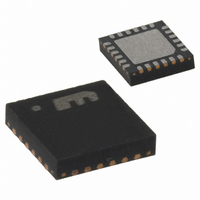
MICRF405YML TR Micrel Inc, MICRF405YML TR Datasheet - Page 11

MICRF405YML TR
Manufacturer Part Number
MICRF405YML TR
Description
868-915 MHz ISM Band Transmitter
Manufacturer
Micrel Inc
Datasheet
1.MICRF405YML_TR.pdf
(46 pages)
Specifications of MICRF405YML TR
Frequency
290MHz ~ 980MHz
Applications
ISM
Modulation Or Protocol
ASK, FSK
Data Rate - Maximum
200 kbps
Power - Output
10dBm
Current - Transmitting
18mA
Data Interface
PCB, Surface Mount
Antenna Connector
PCB, Surface Mount
Voltage - Supply
2.2 V ~ 3.6 V
Operating Temperature
-40°C ~ 125°C
Package / Case
24-MLF®, QFN
Operating Temperature (min)
-40C
Operating Temperature (max)
125C
Operating Temperature Classification
Automotive
Product Depth (mm)
4mm
Product Length (mm)
4mm
Operating Supply Voltage (typ)
2.5/3.3V
Operating Supply Voltage (max)
3.6V
Lead Free Status / RoHS Status
Lead free / RoHS Compliant
Features
-
Memory Size
-
Lead Free Status / Rohs Status
Compliant
Other names
576-1965-2
MICRF405YMLTR
MICRF405YMLTR
MICRF405YMLTR
MICRF405YMLTR
What to write
Field
Address:
R/W bit:
Values:
How to write:
April 2006
Table 6. When writing to Registers having Incremental Addresses, totally 1+n octets are clocked into the MICRF405.
Micrel
• Bring SEN low
• Use SCK and SIO to clock in the 1 + n octets
• Bring SEN high
SCK
SEN
SIO
Comments
7 bit = A6, A5, …A0 (A6 = MSB. A0 = LSB) (address of first byte to write to)
“0” for writing
n* 8 bits =
D7, D6, …D0 (D7 = MSB, D0 = LSB) (written to control reg. with address ”i”)
D7, D6, …D0 (D7 = MSB, D0 = LSB) (written to control reg. with address ”i+1”)
D7, D6, …D0 (D7 = MSB, D0 = LSB) (written to control reg. with address ”I+n-1”)
A6 A5
Register i
address
Figure 3. Writing to n Registers Having Incremental Addresses.
A0 R/W D7 D6
Data to write
into register
i
D0 D7 D6
11
Data to write
into register
i +1
D0
D7 D6
Data to write
into register
i + n - 1
D0
Internal load pulse
generated here
MICRF405
(408) 955-1690
M9999-041906


