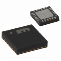
MICRF405YML TR Micrel Inc, MICRF405YML TR Datasheet - Page 10

MICRF405YML TR
Manufacturer Part Number
MICRF405YML TR
Description
868-915 MHz ISM Band Transmitter
Manufacturer
Micrel Inc
Datasheet
1.MICRF405YML_TR.pdf
(46 pages)
Specifications of MICRF405YML TR
Frequency
290MHz ~ 980MHz
Applications
ISM
Modulation Or Protocol
ASK, FSK
Data Rate - Maximum
200 kbps
Power - Output
10dBm
Current - Transmitting
18mA
Data Interface
PCB, Surface Mount
Antenna Connector
PCB, Surface Mount
Voltage - Supply
2.2 V ~ 3.6 V
Operating Temperature
-40°C ~ 125°C
Package / Case
24-MLF®, QFN
Operating Temperature (min)
-40C
Operating Temperature (max)
125C
Operating Temperature Classification
Automotive
Product Depth (mm)
4mm
Product Length (mm)
4mm
Operating Supply Voltage (typ)
2.5/3.3V
Operating Supply Voltage (max)
3.6V
Lead Free Status / RoHS Status
Lead free / RoHS Compliant
Features
-
Memory Size
-
Lead Free Status / Rohs Status
Compliant
Other names
576-1965-2
MICRF405YMLTR
MICRF405YMLTR
MICRF405YMLTR
MICRF405YMLTR
In Figure 2, SIO is changed at positive edges of
SCK. The MICRF405 samples the SIO line at
negative edges. The value of the R/W bits is always
“0” for writing.
Writing to All Registers
Writing to all register can be done at any time. To
get the simplest firmware, always write to all
registers. The price to pay for the simplicity is
increased write-time, which leads to increased time
to change the way the MICRF405 works. If data is
transferred through DATAIN pin write address 0-23
(address 24-29 is don’t care). If data is transferred
through SPI write address 0-28 (Address 29 is only
written
configuration).
What to write
Field
Address:
R/W bit:
Values:
How to write:
Refer to Figure 3. Writing to n Registers Having
Incremental Addresses.
April 2006
Micrel
• Bring SEN low
• Use SCK and SIO to clock in the 25/30 octets
• Bring SEN high
Table 5. When writing to All Registers, totally 25/30 (5 are optional) octets are clocked into the MICRF405.
to
during
SCK
SEN
Comments
‘0000000’ (address of the first register to write to, which is 0)
1
so on for all of the octets.
“0” for writing
SIO
st
Octet: wanted values for ControlRegister0. 2
data
transfer,
A6 A5 A4 A3 A2 A1 A0 R/W D7 D6D5 D4 D3 D2 D1 D0
Register address
Figure 2. Writing to One Address.
not
during
10
Writing to n Registers Having Incremental
Addresses
In addition to entering all bytes, it is also possible to
enter a set of n bytes, starting from address i = “A6,
A5, … A0”. Typical example: Clock in a new set of
frequency dividers (i.e. change the RF frequency).
Registers to be written are located in i, i+1, i+2.
nd
Octet: wanted values for ControlRegister1 and
Data to write
into register
Internal load pulse
generated here
MICRF405
(408) 955-1690
M9999-041906


