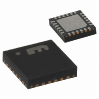
MICRF405YML TR Micrel Inc, MICRF405YML TR Datasheet - Page 13

MICRF405YML TR
Manufacturer Part Number
MICRF405YML TR
Description
868-915 MHz ISM Band Transmitter
Manufacturer
Micrel Inc
Datasheet
1.MICRF405YML_TR.pdf
(46 pages)
Specifications of MICRF405YML TR
Frequency
290MHz ~ 980MHz
Applications
ISM
Modulation Or Protocol
ASK, FSK
Data Rate - Maximum
200 kbps
Power - Output
10dBm
Current - Transmitting
18mA
Data Interface
PCB, Surface Mount
Antenna Connector
PCB, Surface Mount
Voltage - Supply
2.2 V ~ 3.6 V
Operating Temperature
-40°C ~ 125°C
Package / Case
24-MLF®, QFN
Operating Temperature (min)
-40C
Operating Temperature (max)
125C
Operating Temperature Classification
Automotive
Product Depth (mm)
4mm
Product Length (mm)
4mm
Operating Supply Voltage (typ)
2.5/3.3V
Operating Supply Voltage (max)
3.6V
Lead Free Status / RoHS Status
Lead free / RoHS Compliant
Features
-
Memory Size
-
Lead Free Status / Rohs Status
Compliant
Other names
576-1965-2
MICRF405YMLTR
MICRF405YMLTR
MICRF405YMLTR
MICRF405YMLTR
0000000
0001100
0001101
0011001
0011010
0011011
0011100
0011101
April 2006
Data Interface and Data Transfer
There are two main data interfaces; bit-wise and
byte oriented. The bit-wise interface use the DATAIN
(always input to the 405) and DATACLK pin (always
output from the 405). This interface is enabled with
the
synchronous mode is selected and data clock is
provided on the RDY/DATACLK pin. In this mode,
the MICRF405 will sample the bit on the DATAIN pin
on the positive edge of the DATACLK. It is therefore
important that the MCU toggle the DATAIN pin on
negative edge of the DATACLK, See Figure 5. No
packet engine, CRC or Manchester encoding is
available in bit-wise data interface. To select
asynchronous mode set Sync_en=”0”. If VCO
modulation is selected, the DATAIN pin in tri-state
(MCU pin=input) until first bit is about to be
transmitted (see VCO modulation).
If Bit_IO_en=0, the byte wise interface is selected
and data is transferred byte wise through the one
byte buffer (register address 29). The register is
accessed the same way as the other register, as
explained in the previous sections. The only
difference is that it is instantly valid and do not need
any load pulse. This also applies to the SyncID
registers, address 25-28. When writing to address
29, the address counter will not increment which
means several bytes can be written into the buffer
without raising SEN and setting up a new write
session. The RDY/DATACLK pin will provide byte
synchronization. The data byte buffer is ready for
refill on falling edges on RDY. In this mode of data
transfer, Sync_en must be set.
A6..A0
Micrel
DATAIN
DATACLK
Adr
Bit_IO_en=”1”.
LowBatt_level=0
Figure 5. Synchronous Data Interface.
SyncID3_7=1
SyncID2_7=1
SyncID1_7=1
SyncID0_7=1
Bit_IO_en=1
Mode1=0
DATA_7
D7
Manchester_en=0
SyncID3_6=1
SyncID2_6=1
SyncID1_6=1
SyncID0_6=1
LDO_by=0
If
Mode0=1
DATA_6
D6
Sync_en=1
SyncID3_5=1
SyncID2_5=1
SyncID1_5=1
SyncID0_5=1
Sel_CRC1=1
LDO_en1=1
DATA_5
PA2=1
D5
bit-wise
SyncID3_4=0
SyncID2_4=0
SyncID1_4=0
SyncID0_4=0
Sel_CRC0=1
LDO_en0=1
DATA_4
PA1=1
D4
13
Data
The data in the buffer is fed into a packet engine
with an optional CRC calculation and Manchester
encoding. The virtual wire packet structure is shown
in Table 7. The preamble, SyncID field and CRC
field are automatically generated by the packet
engine. The user needs only to enter frame length
and payload for each packet. The preamble bytes
are equal to 10101010, and the number of preamble
bytes are given by 1+Pream_Len[1:0] (D1:D0
ControlRegister13). Next field is the SyncID which is
1-4 bytes long set by the SyncID_Len[1:0] bits. The
content of the SyncID bytes are fully programmable
and specified in the SyncID0-3 bytes. The SyncID0
byte, address 28, is sent first, and the SyncID3 byte,
address 25, is sent last. Refer to Table 8. The frame
length byte follows the SyncID field. It specifies
length of the payload and CRC. Finally, the CRC
field ends the packet. The SelCRC_0 bit specifies
the length of the CRC field. If it is set, a 2 byte ITU-T
CRC (start condition 00h) is calculated of the
payload and sent. If SelCRC_0=0, an 8 bit CCITT
CRC is calculated of the payload and sent. Either
two cases assuming SelCRC_1=1. If SelCRC_1=0,
no CRC is calculated on chip, and the user must
calculate this on the microcontroller and include it in
the payload. A Manchester encoder is available on
chip. It is activated if the Manchester_en bit is set. It
encodes the complete packet. The codes are “10”
for “0” and “01” for “1”. The preamble byte is
automatically set 0 in this mode, as this will produce
the desired 10101010-pattern when Manchester
encoded. Note that on-the-air data rate will be twice
the bit rate set by the FSKClk_K/FSKn or
ASKClk_K/ASKn,
throughput. Because of this, FSKn needs to be
greater than zero if VCO modulation is selected,
Modulation[1:0]<2.
MOD_LDc_en=0
SyncID_Len1=0
SyncID3_3=0
SyncID2_3=0
SyncID1_3=0
SyncID0_3=0
DATA_3
PA0=1
D3
SyncID_Len0=1
PA_FEc_en=0
SyncID3_2=1
SyncID2_2=1
SyncID1_2=1
SyncID0_2=1
ClkOut_en=1
DATA_2
D2
which
Pream_Len1=1
PA_LDc_en=0
SyncID3_1=0
SyncID2_1=0
SyncID1_1=0
SyncID0_1=0
specifies
Sync_en=1
DATA_1
D1
MICRF405
the
Pream_Len0=0
(408) 955-1690
M9999-041906
SyncID3_0=1
SyncID2_0=1
SyncID1_0=1
SyncID0_0=1
Load_en=1
LD_en=1
DATA_0
D0
actual


