CY8C3244LTI-130 Cypress Semiconductor Corp, CY8C3244LTI-130 Datasheet - Page 3
CY8C3244LTI-130
Manufacturer Part Number
CY8C3244LTI-130
Description
PSOC3
Manufacturer
Cypress Semiconductor Corp
Series
PSOC™ 3 CY8C32xxr
Datasheet
1.CY8C3244LTI-130T.pdf
(120 pages)
Specifications of CY8C3244LTI-130
Package / Case
*
Voltage - Supply (vcc/vdd)
1.71 V ~ 5.5 V
Operating Temperature
-40°C ~ 85°C
Speed
50MHz
Number Of I /o
38
Eeprom Size
512 x 8
Core Processor
8051
Program Memory Type
FLASH
Ram Size
2K x 8
Program Memory Size
16KB (16K x 8)
Data Converters
A/D 2x12b, D/A 1x8b
Oscillator Type
Internal
Peripherals
CapSense, DMA, POR, PWM, WDT
Connectivity
EBI/EMI, I²C, LIN, SPI, UART/USART
Core Size
8-Bit
Processor Series
CY8C32
Core
8051
Data Bus Width
32 bit
Data Ram Size
2 KB
Interface Type
I2C, SPI, UART, USB
Maximum Clock Frequency
50 MHz
Number Of Programmable I/os
46
Number Of Timers
4
Operating Supply Voltage
1.71 V to 5.5 V
Maximum Operating Temperature
+ 85 C
Mounting Style
SMD/SMT
Controller Family/series
(8051) PSOC 3
No. Of I/o's
38
Eeprom Memory Size
0.5KB
Ram Memory Size
2KB
Cpu Speed
50MHz
Rohs Compliant
Yes
Lead Free Status / RoHS Status
Lead free / RoHS Compliant
Lead Free Status / RoHS Status
Lead free / RoHS Compliant
Available stocks
Company
Part Number
Manufacturer
Quantity
Price

Part Number:
CY8C3244LTI-130
Manufacturer:
CYPRESS/赛普拉斯
Quantity:
20 000


1. Architectural Overview
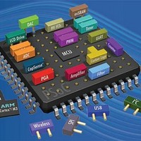
Introducing the CY8C32 family of ultra low-power, flash Programmable System-on-Chip (PSoC
PSoC 3 and 32-bit PSoC 5 platform. The CY8C32 family provides configurable blocks of analog, digital, and interconnect circuitry
around a CPU subsystem. The combination of a CPU with a flexible analog subsystem, digital subsystem, routing, and I/O enables
a high level of integration in a wide variety of consumer, industrial, and medical applications.
Figure 1-1
family. They are:
Document Number: 001-56955 Rev. *K
8051 CPU subsystem
Nonvolatile subsystem
Programming, debug, and test subsystem
Inputs and outputs
Clocking
Power
Digital subsystem
Analog subsystem
0. 5 to 5.5V
( Optional )
32. 7 68 KHz
( Optional )
( Optional )
4- 33 MHz
illustrates the major components of the CY8C32
System Wide
Clocking System
Resources
Power Management
Xtal
Osc
IMO
1.8V LDO
POR and
System
Power
Timer
Wake
Sleep
SMP
WDT
LVD
RTC
ILO
and
Digital Interconnect
8- Bit
Timer
I2C Slave
EEPROM
UART
Figure 1-1. Simplified Block Diagram
LCD Direct
EMIF
Temperature
UDB
UDB
UDB
UDB
CapSense
Universal Digital Block Array ( 24 x UDB)
Sensor
Drive
Quadrature Decoder
Memory System
8- Bit SPI
UDB
UDB
UDB
UDB
FLASH
SRAM
12- Bit SPI
12- Bit PWM
DAC
Logic
UDB
UDB
UDB
UDB
16- Bit
PWM
System Bus
16- Bit PRS
8- Bit
Timer
Digital System
PSoC’s digital subsystem provides half of its unique
configurability. It connects a digital signal from any peripheral to
any pin through the Digital System Interconnect (DSI). It also
provides functional flexibility through an array of small, fast,
low-power UDBs. PSoC Creator provides a library of prebuilt and
tested standard digital peripherals (UART, SPI, LIN, PRS, CRC,
timer, counter, PWM, AND, OR, and so on) that are mapped to
the UDB array. You can also easily create a digital circuit using
boolean primitives by means of graphical design entry. Each
UDB contains programmable array logic (PAL)/programmable
logic device (PLD) functionality, together with a small state
machine engine to support a wide variety of peripherals.
UDB
UDB
UDB
UDB
Analog Interconnect
Logic
Cortex M3
Analog System
8051 or
CPU
UDB
UDB
UDB
UDB
ADC
Del Sig
CPU System
ADC
UDB
UDB
UDB
UDB
Controller
Interrupt
PHUB
DMA
PSoC
Counter
Timer
PWM
4 x
®
) devices, part of a scalable 8-bit
CMP
Program &
2 x
®
Boundary
Debug
Program
Debug &
+
FS USB
-
Master /
Trace
Scan
Slave
3: CY8C32 Family
I2C
2.0
Data Sheet
USB
PHY
Page 3 of 120
22 Ω
Related parts for CY8C3244LTI-130
Image
Part Number
Description
Manufacturer
Datasheet
Request
R

Part Number:
Description:
Manufacturer:
Cypress Semiconductor Corp
Datasheet:
Part Number:
Description:
Manufacturer:
Cypress Semiconductor Corp
Datasheet:
Part Number:
Description:
Manufacturer:
Cypress Semiconductor Corp
Datasheet:
Part Number:
Description:
Manufacturer:
Cypress Semiconductor Corp
Datasheet:
Part Number:
Description:
Manufacturer:
Cypress Semiconductor Corp
Datasheet: