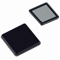
AD8192ACPZ-RL7 Analog Devices Inc, AD8192ACPZ-RL7 Datasheet - Page 5

AD8192ACPZ-RL7
Manufacturer Part Number
AD8192ACPZ-RL7
Description
IC,Telecom Switching Circuit,LLCC,56PIN,PLASTIC
Manufacturer
Analog Devices Inc
Datasheet
1.AD8192ACPZ-RL7.pdf
(28 pages)
Specifications of AD8192ACPZ-RL7
Applications
HDMI, DVI, Receivers
Interface
I²C
Voltage - Supply
3.3V, 5V
Package / Case
56-LFCSP
Mounting Type
Surface Mount
Lead Free Status / RoHS Status
Lead free / RoHS Compliant
ABSOLUTE MAXIMUM RATINGS
Table 4.
Parameter
AVCC to AVEE
DVCC to DVEE
DVEE to AVEE
VTTI
VTTO
AMUXVCC
VREF_AB
VREF_COM
Internal Power Dissipation
High Speed Input Voltage
High Speed Differential
Low Speed Input Voltage
I
Storage Temperature
Operating Temperature
Junction Temperature
ESD HBM Input Pins Only
ESD HBM All Other Pins
2
C Logic Input Voltage
Input Voltage
Range
Range
Rating
3.7 V
3.7 V
±0.3 V
AVCC + 0.6 V
AVCC + 0.6 V
5.5 V
5.5 V
5.5 V
2.41 W
AVCC − 1.4 V < V
2.0 V
DVEE − 0.3 V < V
DVEE − 0.3 V < V
−65°C to +125°C
−40°C to +85°C
150°C
±7 kV
±1.5 kV
IN
IN
IN
< AMUXVCC + 0.6 V
< DVCC + 0.6 V
< AVCC + 0.6 V
Rev. 0 | Page 5 of 28
Stresses above those listed under Absolute Maximum Ratings
may cause permanent damage to the device. This is a stress
rating only; functional operation of the device at these or any
other conditions above those indicated in the operational
section of this specification is not implied. Exposure to absolute
maximum rating conditions for extended periods may affect
device reliability.
THERMAL RESISTANCE
θ
soldered in a four-layer JEDEC circuit board for surface-mount
packages. θ
circuit board with no airflow.
Table 5. Thermal Resistance
Model
56-Lead LFCSP
ESD CAUTION
JA
is specified for the worst-case conditions, that is, a device
JC
is specified for the exposed pad soldered to the
θ
27
JA
θ
2.1
JC
AD8192
Unit
°C/W


