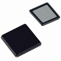
AD8192ACPZ-RL7 Analog Devices Inc, AD8192ACPZ-RL7 Datasheet - Page 24

AD8192ACPZ-RL7
Manufacturer Part Number
AD8192ACPZ-RL7
Description
IC,Telecom Switching Circuit,LLCC,56PIN,PLASTIC
Manufacturer
Analog Devices Inc
Datasheet
1.AD8192ACPZ-RL7.pdf
(28 pages)
Specifications of AD8192ACPZ-RL7
Applications
HDMI, DVI, Receivers
Interface
I²C
Voltage - Supply
3.3V, 5V
Package / Case
56-LFCSP
Mounting Type
Surface Mount
Lead Free Status / RoHS Status
Lead free / RoHS Compliant
AD8192
the amount of parasitic trace capacitance. An example of the
board stackup is shown in Figure 34.
HPD is a dc signal presented by a sink to a source to indicate
that the source EDID is available for reading. The placement of
this signal is not critical, but it should be routed as directly as
possible.
When the AD8192 is powered up, the DDC/CEC inputs of the
selected channel are actively buffered and routed to the outputs,
and the unselected auxiliary inputs are high impedance. When
the AD8192 is powered off, all DDC/CEC inputs are placed in a
high impedance state. This prevents contention on the DDC
bus, enabling a design to include an EDID in front of the AD8192.
Power Supplies
The AD8192 has five separate power supplies referenced to
two separate grounds. The supply/ground pairs are
•
•
•
•
•
•
•
AVCC/AVEE
VTTI/AVEE
VTTO/AVEE
DVCC/DVEE
AMUXVCC/DVEE
VREF_AB/DVEE
VREF_COM/DVEE
SILKSCREEN
LAYER 1: SIGNAL (MICROSTRIP)
PCB DIELECTRIC
LAYER 2: GND (REFERENCE PLANE)
PCB DIELECTRIC
LAYER 3: PWR (REFERENCE PLANE)
PCB DIELECTRIC
LAYER 4: SIGNAL (MICROSTRIP)
SILKSCREEN
Figure 34. Example Board Stackup
3W
RELIEVED UNDERNEATH
REFERENCE LAYER
MICROSTRIP
W
3W
Rev. 0 | Page 24 of 28
The AVCC/AVEE (3.3 V) and DVCC/DVEE (3.3 V) supplies
power the core of the AD8192. The VTTI/AVEE supply (3.3 V)
powers the input termination. Similarly, the VTTO/AVEE supply
(3.3 V) powers the output termination. The AMUXVCC/ DVEE
supply (3.3 V to 5 V) powers the auxiliary multiplexer core. The
VREF_COM and VREF_AB supplies determine the logic levels
on the corresponding DDC buses. For example, if the DDC_COM
bus is using 5 V I
+5 V relative to DVEE. If the DDC_AB buses are using 3.3 V
I
In a typical application, connect all pins labeled AVEE or DVEE
directly to ground. Likewise, connect all pins labeled AVCC,
DVCC, VTTI, or VTTO to 3.3 V, and tie Pin AMUXVCC to
5 V. VREF_AB and VREF_COM can be tied to either 3.3 V
or 5 V, depending on the application. The supplies can also be
powered individually, but care must be taken to ensure that
each stage of the AD8192 is powered correctly.
Power Supply Bypassing
The AD8192 requires minimal supply bypassing. When
powering the supplies individually, place a 0.01 μF capacitor
between each 3.3 V supply pin (AVCC, DVCC, VTTI, and
VTTO) and ground, and place a 0.1 μF capacitor between each
additional supply pin (AMUXVCC, VREF_AB, and VREF_COM)
and ground to filter out supply noise. Generally, place bypass
capacitors near the power pins and connect them directly to the
relevant supplies (without long intervening traces). For example, to
improve the parasitic inductance of the power supply decoupling
capacitors, minimize the trace length between capacitor landing
pads and the vias.
In applications where the AD8192 is powered by a single 3.3 V
supply, it is recommended to use two reference supply planes
and bypass the 3.3 V reference plane to the ground reference
plane with one 220 pF, one 1000 pF, two 0.01 μF, and one 4.7 μF
capacitors. If the AMUXVCC, VREF_AB, and VREF_COM
connections are all powered by a single 5 V supply, it is sufficient
to use a single 0.1 μF to bypass all three connections. The capa-
citors should via down directly to the supply planes and be
placed within a few centimeters of the AD8192.
2
C, then VREF_AB should be connected to +5 V relative to DVEE.
2
C, then VREF_COM should be connected to


