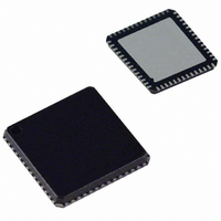
AD8192ACPZ-RL7 Analog Devices Inc, AD8192ACPZ-RL7 Datasheet - Page 20

AD8192ACPZ-RL7
Manufacturer Part Number
AD8192ACPZ-RL7
Description
IC,Telecom Switching Circuit,LLCC,56PIN,PLASTIC
Manufacturer
Analog Devices Inc
Datasheet
1.AD8192ACPZ-RL7.pdf
(28 pages)
Specifications of AD8192ACPZ-RL7
Applications
HDMI, DVI, Receivers
Interface
I²C
Voltage - Supply
3.3V, 5V
Package / Case
56-LFCSP
Mounting Type
Surface Mount
Lead Free Status / RoHS Status
Lead free / RoHS Compliant
AD8192
APPLICATIONS INFORMATION
The AD8192 is an HDMI/DVI switch featuring equalized TMDS
inputs, pre-emphasized TMDS outputs, and buffered auxiliary
signals. It is intended for use as a 2:1 switch in systems with long
cable runs on both the input and/or the output, and is fully
HDMI 1.3a transmit and receive compliant.
PINOUT
By default, the AD8192 is designed to have an HDMI/DVI
receiver pinout at its input and a transmitter pinout at its
output. However, the input/output mapping of the AD8192 is
completely programmable via the serial control interface. This
allows a designer to integrate the AD8192 into virtually any
application without requiring the use of vias on the TMDS
traces in the PCB layout.
In addition to 12 dB of input equalization, the AD8192 provides
up to 6 dB of output pre-emphasis that boosts the output TMDS
DDC_SDA
DDC_SDA
DDC_SCL
DDC_SCL
CLK+
CLK–
CLK+
CLK–
HPD
HPD
CEC
D2+
D2–
D1+
D1–
D0+
D0–
CEC
+5V
D2+
D2–
D1+
D1–
D0+
D0–
+5V
(OPTIONAL)
(OPTIONAL)
0.01uF
0.01uF
PROT.
PROT.
ESD
ESD
EEPROM
EEPROM
2kΩ
2kΩ
EDID
EDID
1kΩ
1kΩ
TMDS
TMDS
kΩ
kΩ
47
47
47
kΩ
47
kΩ
Figure 30. Typical Simplified Schematic
Rev. 0 | Page 20 of 28
IPA3
INA3
IPA2
INA2
IPA1
INA1
IPA0
INA0
HPD_A
SCL_A
SDA_A
CEC_I/O
HPD_B
SCL_B
SDA_B
IPB3
INB3
IPB2
INB2
IPB1
INB1
IPB0
INB0
AD8192
+5V
AMUXVCC
VREF_AB
AVEE, DVEE
VREF_COM
signals and allows the AD8192 to precompensate when driving
long PCB traces or output cables. The net effect of the input
equalization and output pre-emphasis of the AD8192 is that the
AD8192 can compensate for the signal degradation of both input
and output cables; it acts to reopen a closed input data eye and
transmit a full swing HDMI signal to an end receiver.
The AD8192 also provides a distinct advantage in receive-type
applications because it is a fully buffered HDMI/DVI switch;
the AD8192 fully buffers and electrically decouples the outputs
from the inputs for both the TMDS and the auxiliary lines. There-
fore, the effects of any vias placed on the output signal lines are
not seen at the input of the AD8192. The programmable output
terminations also improve signal quality at the output of the
AD8192. Thus, the PCB designer has significantly increased
flexibility in the placement and routing of the output signal path
with the AD8192 over other solutions.
SDA_COM
I2C_ADDR
SCL_COM
I2C_SDA
I2C_SCL
CEC_O/I
OUTP3
OUTN3
OUTP2
OUTN2
OUTP1
OUTN1
OUTP0
OUTN0
+3.3V
AVCC, DVCC
VTTI, VTTO
1kΩ
+3.3V OR +5V
2kΩ
2kΩ
TMDS
+3.3V
2kΩ
2kΩ
D2+
D2–
D1+
D1–
D0+
D0–
CLK+
CLK–
RECEIVER
HDMI
MCU


