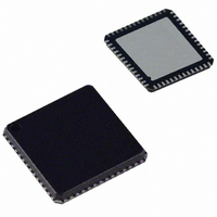
AD8192ACPZ-RL7 Analog Devices Inc, AD8192ACPZ-RL7 Datasheet - Page 12

AD8192ACPZ-RL7
Manufacturer Part Number
AD8192ACPZ-RL7
Description
IC,Telecom Switching Circuit,LLCC,56PIN,PLASTIC
Manufacturer
Analog Devices Inc
Datasheet
1.AD8192ACPZ-RL7.pdf
(28 pages)
Specifications of AD8192ACPZ-RL7
Applications
HDMI, DVI, Receivers
Interface
I²C
Voltage - Supply
3.3V, 5V
Package / Case
56-LFCSP
Mounting Type
Surface Mount
Lead Free Status / RoHS Status
Lead free / RoHS Compliant
AD8192
THEORY OF OPERATION
The primary function of the AD8192 is to switch one of two
(HDMI or DVI) single link sources to one output. Each
HDMI/DVI link consists of four differential, high speed
channels and four auxiliary single-ended, low speed control
signals. The high speed channels include a data-word clock
and three transition minimized differential signaling (TMDS)
data channels running at 10× the data-word clock frequency
for data rates up to 2.25 Gbps. The low speed control signals
include the display data channel (DDC) bus (SDA and SCL),
the consumer electronics control (CEC) line, and the hot plug
detect (HPD) signal.
All four high speed TMDS channels are identical; that is, the
pixel clock can be run on any of the four TMDS channels.
Transmit and receive channel compensation is provided for
the high speed channels where the user can (manually) select
among a number of fixed settings.
The AD8192 isolates and buffers the DDC bus. It additionally
isolates and buffers the CEC line and includes integrated pull-
ups for the CEC line. The AD8192 also pulses the HPD signal
low upon channel switching.
The AD8192 has I
grammable I
AD8192 is 0b100100X. The least significant bit, represented
by X in the address, is set by tying the I2C_ADDR pin to either
3.3 V (for the value X = 1) or to 0 V (for X = 0).
INPUT CHANNELS
Each high speed input differential pair terminates to the 3.3 V
VTTI power supply through a pair of single-ended 50 Ω on-
chip resistors, as shown in Figure 25. The state of the input
terminations can be configured automatically or programmed
manually through the serial control interface. The termination
state is placed in the automatic mode by programming 0 in the
RX_TO bit of the receiver settings register. In the automatic
mode, the selected input has all terminations enabled, and the
deselected input has all input terminations disabled. This state
is automatically updated upon channel switching. In the manual
mode, 1 is programmed into the RX_TO bit of the receiver
settings register, and the state of each individual input termi-
nation is set by programming the associated RX_PT bits in the
input termination control register.
The input equalizer can be manually configured to provide two
different levels of high frequency boost: 6 dB or 12 dB. The
equalizer level defaults to 12 dB after reset. The user can
individually program the equalization level of the eight high
speed input channels by selectively setting the associated RX_EQ
bits in the receive equalizer register. No specific cable length is
suggested for a particular equalization setting because cable
performance varies widely among manufacturers; however, in
general, the equalization of the AD8192 can be set to 12 dB
without degrading the signal integrity, even for short input cables.
2
C slave addresses. The I
2
C serial programming with two user pro-
2
C slave address of the
Rev. 0 | Page 12 of 28
OUTPUT CHANNELS
Each high speed output differential pair is terminated to the
+3.3 V VTTO power supply through a pair of 50 Ω on-chip
resistors, as shown in Figure 26. This termination is user-
selectable; it can be turned on or off by programming the
TX_PTO bit of the transmitter settings register.
The output termination resistors of the AD8192 back terminate
the output TMDS transmission lines. These back terminations,
as recommended in the HDMI 1.3a specification, act to absorb
reflections from impedance discontinuities on the output traces,
improving the signal integrity of the output traces and adding
flexibility to how the output traces can be routed. For example,
interlayer vias can be used to route the AD8192 TMDS outputs
on multiple layers of the PCB without severely degrading the
quality of the output signal.
The output has a disable feature that places the outputs in
tristate mode (HS_EN bit of the high speed device modes
register). Bigger wire-OR’ e d arrays can be constructed using
the AD8192 in this mode.
The AD8192 requires output termination resistors when the
high speed outputs are enabled. Termination can be internal
and/or external. The internal terminations of the AD8192 are
enabled by programming the TX_PTO bit of the transmitter
settings register (the default upon reset). External terminations
can be provided either by on-board resistors or by the input
termination resistors of an HDMI/DVI receiver. If both the
internal terminations are enabled and external terminations are
present, set the output current level to 20 mA by programming
the TX_OCL bit of the transmitter settings register (the default
upon reset). If only external terminations are provided (if the
internal terminations are disabled), set the output current level
Figure 26. High Speed Output Simplified Schematic
OP
Figure 25. High Speed Input Simplified Schematic
IN
IP
AVEE
DISABLE
VTTI
50Ω
VTTO
AVEE
I
50Ω
OUT
50Ω
50Ω
CABLE
ON
EQ
PROT.
ESD


