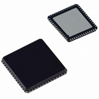
AD8192ACPZ-RL7 Analog Devices Inc, AD8192ACPZ-RL7 Datasheet - Page 14

AD8192ACPZ-RL7
Manufacturer Part Number
AD8192ACPZ-RL7
Description
IC,Telecom Switching Circuit,LLCC,56PIN,PLASTIC
Manufacturer
Analog Devices Inc
Datasheet
1.AD8192ACPZ-RL7.pdf
(28 pages)
Specifications of AD8192ACPZ-RL7
Applications
HDMI, DVI, Receivers
Interface
I²C
Voltage - Supply
3.3V, 5V
Package / Case
56-LFCSP
Mounting Type
Surface Mount
Lead Free Status / RoHS Status
Lead free / RoHS Compliant
AD8192
AUXILIARY MULTIPLEXER
The auxiliary (low speed) lines provide switching and buffering
for the DDC bus and buffering for the CEC line. The DDC
buffers are bidirectional and fully support arbitration, clock
synchronization, and other relevant features of a standard mode
I
on-chip pull-up resistors.
The HPD lines going into the AD8192 are normally high
impedance but are pulled low for greater than 100 ms when
a channel switch occurs.
The user has the option of slaving the auxiliary line switch
select to the high speed switch select by programming the
AUX_LK bit of the auxiliary device register. This causes the
auxiliary input channel to switch automatically when the user
programs the HS_CH bit of the high speed modes register.
The unselected auxiliary inputs of the AD8192 are placed into a
high impedance mode when the device is powered up and the
DDC inputs of the AD8192 are high impedance when the
device is powered off. This prevents contention on the DDC bus,
enabling a design to include an EDID upstream of the AD8192.
DDC LOGIC LEVELS
The AD8192 supports the use of flexible (3.3 V, 5 V) logic levels
on the DDC bus. The logic level for the DDC_A and DDC_B
buses are set by the voltage on VREF_AB, and the logic level
for the DDC_COM bus is set by the voltage on VREF_COM.
For example, if the DDC_COM bus is using 5 V I
VREF_COM power supply pin should be connected to a +5 V
power supply. If the DDC_AB buses are using 3.3 V I
the VREF_AB power supply pin should be connected to a
+3.3 V power supply.
2
C bus. The CEC buffer is bidirectional and includes integrated
2
C, then the
2
C, then
Rev. 0 | Page 14 of 28
INPUT/OUTPUT MAPPING CONTROL
The input/output mapping of the AD8192 is completely
programmable. This allows a designer to integrate the AD8192
into virtually any application without requiring the use of vias
on the TMDS traces in the PCB layout.
The user can independently control the input/output mapping
of the TMDS channels for both Source A and Source B by
programming the A[3:0]_HS_MAP[0:1] bits of the Source A
input/output mapping register and the B[3:0]_HS_MAP[0:1]
bits of the Source B input/output mapping register, respectively.
The user can independently control the polarity of the eight
input channels by programming the A_SG and B_SG bits of the
source sign select register. This allows a designer to invert the
order of the p and n signals of a given TMDS pair inside the
AD8192 instead of on the PCB.


