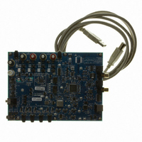
CDB42L52 Cirrus Logic Inc, CDB42L52 Datasheet - Page 77

CDB42L52
Manufacturer Part Number
CDB42L52
Description
Eval Bd LP Codec W/Class D Spkr Driver
Manufacturer
Cirrus Logic Inc
Specifications of CDB42L52
Main Purpose
Audio, CODEC
Embedded
Yes, FPGA / CPLD
Utilized Ic / Part
CS42L52
Primary Attributes
4 Stereo Audio Inputs, Stereo Line and Speaker Outputs, S/PDIF Inputs and Outputs
Secondary Attributes
GUI, I2C, SPI, USB Interfaces
Description/function
Audio CODECs
Operating Supply Voltage
5 V
Product
Audio Modules
Lead Free Status / RoHS Status
Contains lead / RoHS non-compliant
For Use With/related Products
CS42L52
Lead Free Status / RoHS Status
Contains lead / RoHS non-compliant
Other names
598-1505
DS680F1
9. PCB LAYOUT CONSIDERATIONS
9.1
9.2
Power Supply, Grounding
As with any high-resolution converter, the CS42L52 requires careful attention to power supply and ground-
ing arrangements if its potential performance is to be realized.
ed power arrangements, with VA and VHP connected to clean supplies VD, which powers the digital
circuitry, may be run from the system logic supply. Alternatively, VD may be powered from the analog supply
via a ferrite bead. In this case, no additional devices should be powered from VD.
Extensive use of power and ground planes, ground plane fill in unused areas and surface mount decoupling
capacitors are recommended. Decoupling capacitors should be as close to the pins of the CS42L52 as pos-
sible. The low value ceramic capacitor should be closest to the pin and should be mounted on the same
side of the board as the CS42L52 to minimize inductance effects.
All signals, especially clocks, should be kept away from the FILT+ and VQ pins in order to avoid unwanted
coupling into the modulators. The FILT+ and VQ decoupling capacitors, particularly the 0.1 µF, must be po-
sitioned to minimize the electrical path from FILT+ and AGND. The CDB42L52 evaluation board demon-
strates the optimum layout and power supply arrangements.
QFN Thermal Pad
The CS42L52 is available in a compact QFN package. The underside of the QFN package reveals a large
metal pad that serves as a thermal relief to provide for maximum heat dissipation. This pad must mate with
an equally dimensioned copper pad on the PCB and must be electrically connected to ground. A series of
vias should be used to connect this copper pad to one or more larger ground planes on other PCB layers.
In split ground systems, it is recommended that this thermal pad be connected to AGND for best perfor-
mance. The CS42L52 evaluation board demonstrates the optimum thermal pad and via configuration.
5/13/08
Figure 1 on page 10
shows the recommend-
CS42L52
77


