CDB42L52 Cirrus Logic Inc, CDB42L52 Datasheet - Page 15
CDB42L52
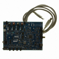
Manufacturer Part Number
CDB42L52
Description
Eval Bd LP Codec W/Class D Spkr Driver
Manufacturer
Cirrus Logic Inc
Specifications of CDB42L52
Main Purpose
Audio, CODEC
Embedded
Yes, FPGA / CPLD
Utilized Ic / Part
CS42L52
Primary Attributes
4 Stereo Audio Inputs, Stereo Line and Speaker Outputs, S/PDIF Inputs and Outputs
Secondary Attributes
GUI, I2C, SPI, USB Interfaces
Description/function
Audio CODECs
Operating Supply Voltage
5 V
Product
Audio Modules
Lead Free Status / RoHS Status
Contains lead / RoHS non-compliant
For Use With/related Products
CS42L52
Lead Free Status / RoHS Status
Contains lead / RoHS non-compliant
Other names
598-1505


DS680F1
ANALOG OUTPUT CHARACTERISTICS (COMMERCIAL - CNZ)
Test conditions (unless otherwise specified): Input test signal is a full-scale 997 Hz sine wave; All Supplies = VA; T
Sample Frequency = 48 kHz; Measurement bandwidth is 20 Hz to 20 kHz; Test load R
(see
ization Settings” on page 37
R
Dynamic Range
18- to 24-Bit
16-Bit
Total Harmonic Distortion + Noise
18- to 24-Bit
16-Bit
R
Dynamic Range
18- to 24-Bit
16-Bit
Total Harmonic Distortion + Noise
18- to 24-Bit
16-Bit
Other Characteristics for R
Output Parameters
(Note 7)
Full-scale Output Voltage (2•G•MI•VA)
Full-scale Output Power
Interchannel Isolation (1 kHz)
Speaker Amp to HP Amp Isolation
Interchannel Gain Mismatch
Gain Drift
AC Load Resistance (R
Load Capacitance (C
L
L
= 10 k
= 16
Figure
6. One-half LSB of triangular PDF dither is added to data.
7. Full-scale output voltage and power is determined by the gain setting, G, in register
Ω
Ω
2); Test load R
Gain” on page
audio signal approaches full-scale, maximum power output, as shown in
Parameters
L
)
L
)
(Note 7)
L
= 16 Ω, C
written on power up.
L
51. High gain settings at certain VA and VHP supply levels may cause clipping when the
= 16
Analog Gain Multiplier (G)
(Note 6)
Modulation Index (MI)
Ω
L
or 10 k
= 10 pF (see
(Note 7)
unweighted
unweighted
unweighted
unweighted
Ω
A-weighted
A-weighted
A-weighted
A-weighted
(Note 8)
(Note 8)
-20 dB
-60 dB
-20 dB
-60 dB
-20 dB
-60 dB
-20 dB
-60 dB
10 kΩ
Figure
16 Ω
0 dB
0 dB
0 dB
0 dB
Refer to Table
tics” on page 20
Refer to Table
page 19
2) for the headphone output; HP_GAIN[2:0] = 011;
5/13/08
Min
92
89
92
89
16
-
-
-
-
-
-
-
-
-
-
-
-
-
-
-
-
-
-
-
-
-
-
-
-
VA = 2.5 V
0.6787
0.6047
±100
Typ
-86
-75
-35
-86
-73
-33
-75
-75
-35
-75
-73
-33
0.1
98
95
96
93
98
95
96
93
80
95
80
“Line Output Voltage Level Characteris-
-
-
“Headphone Output Power Characteristics” on
Max
0.25
150
-80
-29
-69
-29
-
-
-
-
-
-
-
-
-
-
-
-
-
-
-
-
-
-
-
-
-
-
-
L
= 10 kΩ, C
Min
89
86
89
86
16
-
-
-
-
-
-
-
-
-
-
-
-
-
-
-
-
-
-
-
-
-
-
-
-
Figures 22
VA = 1.8 V
L
0.6787
0.6047
= 10 pF for the line output
±100
Typ
-88
-72
-32
-88
-70
-30
-75
-72
-32
-75
-70
-30
0.1
95
92
93
90
95
92
93
90
80
93
80
-
-
“Headphone Analog
-
25 on page
“Required Initial-
Max
0.25
150
-82
-26
-69
-26
CS42L52
-
-
-
-
-
-
-
-
-
-
-
-
-
-
-
-
-
-
-
-
-
-
-
A
= +25°C;
ppm/°C
Unit
Vpp
dB
dB
dB
dB
dB
dB
dB
dB
dB
dB
dB
dB
dB
dB
dB
dB
dB
dB
dB
dB
dB
dB
dB
dB
pF
Ω
75.
15
Related parts for CDB42L52
Image
Part Number
Description
Manufacturer
Datasheet
Request
R

Part Number:
Description:
Development Kit
Manufacturer:
Cirrus Logic Inc
Datasheet:
Part Number:
Description:
Development Kit
Manufacturer:
Cirrus Logic Inc
Datasheet:


Part Number:
Description:
High-efficiency PFC + Fluorescent Lamp Driver Reference Design
Manufacturer:
Cirrus Logic Inc
Datasheet:
Part Number:
Description:
Development Kit
Manufacturer:
Cirrus Logic Inc
Datasheet:
Part Number:
Description:
Development Kit
Manufacturer:
Cirrus Logic Inc
Datasheet:

Part Number:
Description:
Development Kit
Manufacturer:
Cirrus Logic Inc
Datasheet:
Part Number:
Description:
Development Kit
Manufacturer:
Cirrus Logic Inc
Datasheet:
Part Number:
Description:
Development Kit
Manufacturer:
Cirrus Logic Inc
Datasheet:
Part Number:
Description:
Development Kit
Manufacturer:
Cirrus Logic Inc
Datasheet:

Part Number:
Description:
EVALUATION BOARD FOR CS8427
Manufacturer:
Cirrus Logic Inc
Datasheet:

Part Number:
Description:
BOARD EVAL FOR CS8416 RCVR
Manufacturer:
Cirrus Logic Inc
Datasheet:

Part Number:
Description:
EVALUATION BOARD FOR CS8420
Manufacturer:
Cirrus Logic Inc
Datasheet:

Part Number:
Description:
KIT DEVELOPMENT EP9315 ARM9
Manufacturer:
Cirrus Logic Inc
Datasheet:

Part Number:
Description:
KIT DEVELOPMENT EP9302 ARM9
Manufacturer:
Cirrus Logic Inc
Datasheet: