CDB42L52 Cirrus Logic Inc, CDB42L52 Datasheet
CDB42L52
Specifications of CDB42L52


Related parts for CDB42L52


CDB42L52 Summary of contents
Page 1
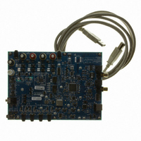
... MCLK Oscillator (socket) http://www.cirrus.com Description Using the CDB42L52 evaluation board is an ideal way to evaluate the CS42L52 CODEC. Use of the board re- quires an analog/digital signal source, an analyzer and power supplies. A Windows PC-compatible computer is also needed in order to configure the CS42L52 and the board functionality. ...
Page 2
... Figure 10.Micro & FPGA Control (Schematic Sheet 3) ............................................................................. 19 Figure 11.Power (Schematic Sheet 4) ...................................................................................................... 20 Figure 12.Silk Screen ................................................................................................................................ 21 Figure 13.Top-Side Layer ......................................................................................................................... 22 Figure 14.GND (Layer 2) ........................................................................................................................... 23 Figure 15.Power (Layer 3) ........................................................................................................................ 24 Figure 16.Bottom Side Layer .................................................................................................................... 25 LIST OF TABLES Table 1. System Connections ................................................................................................................... 13 Table 2. Jumper Settings .......................................................................................................................... 14 2 CDB42L52 DS680DB1 ...
Page 3
... SYSTEM OVERVIEW The CDB42L52 platform provides analog and digital interfaces to the CS42L52 and allows for external DSP and ® I²C interconnect. On board power regulators are provided so that only an external +5 V power supply is neces- sary. Board configuration is done using the Windows PC-compatible GUI to read/write device registers. An FPGA on the board helps make clock/data routing and CS42L52 configuration easy ...
Page 4
... CS8406 data sheet. The CS8406 converts the PCM data generated by the CS42L52 to the standard S/PDIF data stream and routes this signal to the optical and RCA connectors on the CDB42L52. Selections are made by using the “Board Configuration” tab of the Cirrus FlexGUI software. ...
Page 5
... FlexGUI software enables the CDB42L52. Note: The USB port connection also provides DC power to the board (except for VP). The minimum current required is approximately 300 mA. It may, therefore, be nec- essary to connect the CDB42L52 directly to the USB port on the PC as opposed to a hub or keyboard port where current may be limited. ...
Page 6
... Set up the CS42L52 in the “CODEC Configuration”, “Analog Input Volume”, “DSP Engine” and “Analog and PWM Output Volume” tab as desired. 8. Begin evaluating the CS42L52. For quick set-up, the CDB42L52 may, alternatively, be configured by loading a predefined sample script file the File menu, click "Restore Board Registers..." 10. Browse to Boards\CDB42L52\Scripts\. ...
Page 7
... Board Configuration Tab The “Board Configuration” tab provides high-level control of signal routing on the CDB42L52. This tab also includes basic controls that allow “quick setup” number of simple board configurations. Status text de- tailing the CODEC’s specific configuration appears directly below the associated control. This text may change depending on the setting of the associated control ...
Page 8
... Serial Port Configuration - Controls for all settings related to the serial I/O data and clocks on the board. DAC Configuration - Control for the signal source to the DAC and analog output mux. Update - Reads all registers in the CS42L52 and reflects the current values in the GUI. Reset - Resets the CS42L52. 8 Figure 2. CODEC Configuration Tab CDB42L52 DS680DB1 ...
Page 9
... Analog Volume Control - Analog volume controls and adjustments (PGA and MIC amps). Noise Gate Configuration - All configuration settings for the noise gate. Update - Reads all registers in the CS42L52 and reflects the current values in the GUI. Reset - Resets the CS42L52. DS680DB1 Figure 3. ADC Channel Volume Tab CDB42L52 9 ...
Page 10
... Tone Control - Bass and treble volume controls and filter corner frequencies. Beep Generator - On/Off time, frequency, volume, mix and repeat beep functions. Update - Reads all registers in the CS42L52 and reflects the current values in the GUI. Reset - Resets the CS42L52. 10 Figure 4. ADC Channel Volume Tab CDB42L52 DS680DB1 ...
Page 11
... PWM Output - Volume, mute, power down and other functional controls for the PWM speaker outputs. Temperature and Battery Monitor/Control - Battery Compensation, Thermal Foldback, Temperature Shut- down and Battery Monitor for the PWM/Speaker outputs. DS680DB1 Figure 5. Analog and PWM Output Volume Tab CDB42L52 11 ...
Page 12
... The user can change the register con- tents by using the push-buttons, by selecting a particular bit and typing in the new bit value or by selecting the register in the map and typing in a new hex value. 12 Figure 6. Register Maps Tab - CS42L52 CDB42L52 DS680DB1 ...
Page 13
... Binding Post speaker outputs. Output Stereo 1/8” jack for DAC outputs. When headphones are plugged Connect, this output is disconnected. Output Stereo headphone jack for DAC outputs. Input/Output Digital Audio and Clocks to/from a DSP device. Table 1. System Connections CDB42L52 SIGNAL PRESENT 13 ...
Page 14
... SPKOUTA-/+ SHUNTED *OPEN for SPKOUTB-/+ SHUNTED Table 2. Jumper Settings CDB42L52 FUNCTION SELECTED Voltage source is +1.8 V regulator. Voltage source is +2.5 V regulator. Voltage source is +3.3 V regulator. Voltage source is +1.8 V regulator. Voltage source is +2.5 V regulator. . Voltage source is +1.8 V regulator. Voltage source is +2.5 V regulator. . ...
Page 15
... Filtered HP/LINE_OUTA to HP/Line Jack Non-filtered HP/LINE_OUTA to HP/Line Jack Filtered HP/LINE_OUTA to HP/Line Jack FPGA generated HP_DET signal selected Jack generated HP_DET signal selected External +5 V power USB generated +5 V power External VP power Battery VP power 1.65 V select 1.8 V select. Table 2. Jumper Settings CDB42L52 *Default factory settings 15 ...
Page 16
CDB42L51 BLOCK DIAGRAM Software Mode Control Port Reset Figure 10 on page 19 S/PDIF I/O (CS8406 + CS8416) Figure 9 on page 18 Clk/Data SRC Figure 9 on page 18 Figure 9 on page 18 I²C/SPI Header Figure 8 on ...
Page 17
CDB42L51 SCHEMATICS Figure 8. CS42L52 & Analog I/O (Schematic Sheet 1) ...
Page 18
Figure 9. S/PDIF & Digital Interface (Schematic Sheet 2) ...
Page 19
Figure 10. Micro & FPGA Control (Schematic Sheet 3) ...
Page 20
Figure 11. Power (Schematic Sheet 4) ...
Page 21
CDB42L51 LAYOUT Figure 12. Silk Screen ...
Page 22
Figure 13. Top-Side Layer ...
Page 23
Figure 14. GND (Layer 2) ...
Page 24
Figure 15. Power (Layer 3) ...
Page 25
Figure 16. Bottom Side Layer ...
Page 26
... Cirrus Logic, Cirrus, and the Cirrus Logic logo designs are trademarks of Cirrus Logic, Inc. All other brand and product names in this document may be trademarks or service marks of their respective owners. I² registered trademark of Philips Semiconductor. Windows is a registered trademark of Microsoft Corporation. 26 Changes www.cirrus.com. CDB42L52 DS680DB1 ...