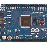
A000047 Arduino, A000047 Datasheet - Page 77
A000047
Manufacturer Part Number
A000047
Description
MCU, MPU & DSP Development Tools Mega2560
Manufacturer
Arduino
Series
-r
Type
MCUr
Specifications of A000047
Processor To Be Evaluated
ATmega2560
Interface Type
USB, I2C, SPI
Dimensions
4 in x 2.1 in
Operating Supply Voltage
5 V
Contents
Board
Lead Free Status / RoHS Status
Lead free / RoHS Compliant
For Use With/related Products
ATmega2560


2549M–AVR–09/10
Table 12-2
ure 12-5 on page 76
generated internally in the modules having the alternate function.
Table 12-2.
The following subsections shortly describe the alternate functions for each port, and relate the
overriding signals to the alternate function. Refer to the alternate function description for further
details.
Signal Name
DIEOE
DIEOV
PUOE
DDOE
DDOV
PUOV
PVOE
PVOV
PTOE
AIO
DI
summarizes the function of the overriding signals. The pin and port indexes from
Generic Description of Overriding Signals for Alternate Functions
Pull-up Override
Pull-up Override
Override Enable
Override Enable
Override Enable
Enable Override
Enable Override
Override Value
Override Value
Data Direction
Data Direction
Input/Output
Digital Input
Digital Input
Digital Input
Port Toggle
Full Name
Port Value
Port Value
are not shown in the succeeding tables. The overriding signals are
Enable
Enable
Analog
Value
Value
ATmega640/1280/1281/2560/2561
If this signal is set, the pull-up enable is controlled by the PUOV
If this signal is set, the Output Driver Enable is controlled by the
DIEOV signal. If this signal is cleared, the Digital Input Enable is
value is controlled by the PVOV signal. If PVOE is cleared, and
the Output Driver is enabled, the port Value is controlled by the
clock source, the module with the alternate function will use its
This is the Analog Input/output to/from alternate functions. The
This is the Digital Input to alternate functions. In the figure, the
If PVOE is set, the port value is set to PVOV, regardless of the
If PUOE is set, the pull-up is enabled/disabled when PUOV is
before the synchronizer. Unless the Digital Input is used as a
If this signal is set and the Output Driver is enabled, the port
set/cleared, regardless of the setting of the DDxn, PORTxn,
DIEOV is set/cleared, regardless of the MCU state (Normal
If DDOE is set, the Output Driver is enabled/disabled when
signal is connected directly to the pad, and can be used bi-
signal. If this signal is cleared, the pull-up is enabled when
DDOV is set/cleared, regardless of the setting of the DDxn
If this bit is set, the Digital Input Enable is controlled by the
If DIEOE is set, the Digital Input is enabled/disabled when
signal is connected to the output of the schmitt trigger but
DDOV signal. If this signal is cleared, the Output driver is
determined by MCU state (Normal mode, sleep mode).
If PTOE is set, the PORTxn Register bit is inverted.
setting of the PORTxn Register bit.
enabled by the DDxn Register bit.
{DDxn, PORTxn, PUD} = 0b010.
and PUD Register bits.
PORTxn Register bit.
mode, sleep mode).
own synchronizer.
Description
directionally.
Register bit.
Fig-
77
Related parts for A000047
Image
Part Number
Description
Manufacturer
Datasheet
Request
R

Part Number:
Description:
Daughter Cards & OEM Boards ARDUINO UNO PROTO PCB REV 3
Manufacturer:
Arduino
Part Number:
Description:
Daughter Cards & OEM Boards ARDUINO SHIELD PROTO KIT REV 3
Manufacturer:
Arduino
Part Number:
Description:
Daughter Cards & OEM Boards ARDUINO MEGA PROTO KIT REV 3
Manufacturer:
Arduino
Part Number:
Description:
Daughter Cards & OEM Boards ARDUINO MEGA PROTO PCB REV 3
Manufacturer:
Arduino
Part Number:
Description:
Development Boards & Kits - AVR ARDUINO STARTER KIT W/ UNO REV3
Manufacturer:
Arduino
Part Number:
Description:
RF Development Tools ARDUINO SHIELD WIRELESS PROTO
Manufacturer:
Arduino
Datasheet:
Part Number:
Description:
RF Development Tools ARDUINO SHIELD WIRELESS WITH SD
Manufacturer:
Arduino
Datasheet:

Part Number:
Description:
Development Software Getting started w/Arduino
Manufacturer:
Arduino

Part Number:
Description:
Ethernet Modules & Development Tools Ethernet Shield for Arduino
Manufacturer:
Arduino

Part Number:
Description:
MCU, MPU & DSP Development Tools LilyPad Arduino Main Board
Manufacturer:
Arduino

Part Number:
Description:
ARDUINO NANO Board
Manufacturer:
Arduino
Datasheet:
Part Number:
Description:
Ethernet Modules & Development Tools ETHERNET SHEILD PoE FOR ARDUINO
Manufacturer:
Arduino
Datasheet:

Part Number:
Description:
ATMEGA328 MCU IC W/ Arduino UNO Bootloader
Manufacturer:
Arduino
Datasheet:
Part Number:
Description:
Memory Cards MICRO SD CARD 1GB WITH SD ADAPTER
Manufacturer:
Arduino