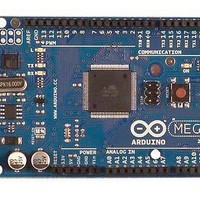
A000047 Arduino, A000047 Datasheet - Page 296
A000047
Manufacturer Part Number
A000047
Description
MCU, MPU & DSP Development Tools Mega2560
Manufacturer
Arduino
Series
-r
Type
MCUr
Specifications of A000047
Processor To Be Evaluated
ATmega2560
Interface Type
USB, I2C, SPI
Dimensions
4 in x 2.1 in
Operating Supply Voltage
5 V
Contents
Board
Lead Free Status / RoHS Status
Lead free / RoHS Compliant
For Use With/related Products
ATmega2560


26. JTAG Interface and On-chip Debug System
26.1
26.2
2549M–AVR–09/10
Features
Overview
•
•
•
•
•
•
The AVR IEEE std. 1149.1 compliant JTAG interface can be used for
•
•
•
A brief description is given in the following sections. Detailed descriptions for Programming via
the JTAG interface, and using the Boundary-scan Chain can be found in the sections
ming via the JTAG Interface” on page 354
302, respectively. The On-chip Debug support is considered being private JTAG instructions,
and distributed within ATMEL and to selected third party vendors only.
Figure 26-1 on page 297
system. The TAP Controller is a state machine controlled by the TCK and TMS signals. The TAP
Controller selects either the JTAG Instruction Register or one of several Data Registers as the
scan chain (Shift Register) between the TDI – input and TDO – output. The Instruction Register
holds JTAG instructions controlling the behavior of a Data Register.
The ID-Register, Bypass Register, and the Boundary-scan Chain are the Data Registers used
for board-level testing. The JTAG Programming Interface (actually consisting of several physical
and virtual Data Registers) is used for serial programming via the JTAG interface. The Internal
Scan Chain and Break Point Scan Chain are used for On-chip debugging only.
JTAG (IEEE std. 1149.1 Compliant) Interface
Boundary-scan Capabilities According to the IEEE std. 1149.1 (JTAG) Standard
Debugger Access to:
Extensive On-chip Debug Support for Break Conditions, Including
Programming of Flash, EEPROM, Fuses, and Lock Bits through the JTAG Interface
On-chip Debugging Supported by AVR Studio
– All Internal Peripheral Units
– Internal and External RAM
– The Internal Register File
– Program Counter
– EEPROM and Flash Memories
– AVR Break Instruction
– Break on Change of Program Memory Flow
– Single Step Break
– Program Memory Break Points on Single Address or Address Range
– Data Memory Break Points on Single Address or Address Range
Testing PCBs by using the JTAG Boundary-scan capability.
Programming the non-volatile memories, Fuses and Lock bits.
On-chip debugging.
shows a block diagram of the JTAG interface and the On-chip Debug
ATmega640/1280/1281/2560/2561
and
®
“IEEE 1149.1 (JTAG) Boundary-scan” on page
“Program-
296
Related parts for A000047
Image
Part Number
Description
Manufacturer
Datasheet
Request
R

Part Number:
Description:
Daughter Cards & OEM Boards ARDUINO UNO PROTO PCB REV 3
Manufacturer:
Arduino
Part Number:
Description:
Daughter Cards & OEM Boards ARDUINO SHIELD PROTO KIT REV 3
Manufacturer:
Arduino
Part Number:
Description:
Daughter Cards & OEM Boards ARDUINO MEGA PROTO KIT REV 3
Manufacturer:
Arduino
Part Number:
Description:
Daughter Cards & OEM Boards ARDUINO MEGA PROTO PCB REV 3
Manufacturer:
Arduino
Part Number:
Description:
Development Boards & Kits - AVR ARDUINO STARTER KIT W/ UNO REV3
Manufacturer:
Arduino
Part Number:
Description:
RF Development Tools ARDUINO SHIELD WIRELESS PROTO
Manufacturer:
Arduino
Datasheet:
Part Number:
Description:
RF Development Tools ARDUINO SHIELD WIRELESS WITH SD
Manufacturer:
Arduino
Datasheet:

Part Number:
Description:
Development Software Getting started w/Arduino
Manufacturer:
Arduino

Part Number:
Description:
Ethernet Modules & Development Tools Ethernet Shield for Arduino
Manufacturer:
Arduino

Part Number:
Description:
MCU, MPU & DSP Development Tools LilyPad Arduino Main Board
Manufacturer:
Arduino

Part Number:
Description:
ARDUINO NANO Board
Manufacturer:
Arduino
Datasheet:
Part Number:
Description:
Ethernet Modules & Development Tools ETHERNET SHEILD PoE FOR ARDUINO
Manufacturer:
Arduino
Datasheet:

Part Number:
Description:
ATMEGA328 MCU IC W/ Arduino UNO Bootloader
Manufacturer:
Arduino
Datasheet:
Part Number:
Description:
Memory Cards MICRO SD CARD 1GB WITH SD ADAPTER
Manufacturer:
Arduino