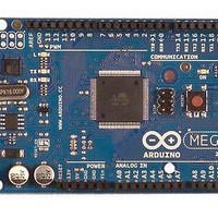
A000047 Arduino, A000047 Datasheet - Page 308
A000047
Manufacturer Part Number
A000047
Description
MCU, MPU & DSP Development Tools Mega2560
Manufacturer
Arduino
Series
-r
Type
MCUr
Specifications of A000047
Processor To Be Evaluated
ATmega2560
Interface Type
USB, I2C, SPI
Dimensions
4 in x 2.1 in
Operating Supply Voltage
5 V
Contents
Board
Lead Free Status / RoHS Status
Lead free / RoHS Compliant
For Use With/related Products
ATmega2560


27.6
27.6.1
27.6.2
27.7
27.8
2549M–AVR–09/10
Boundary-scan Related Register in I/O Memory
ATmega640/1280/1281/2560/2561 Boundary-scan Order
Boundary-scan Description Language Files
MCUCR – MCU Control Register
MCUSR – MCU Status Register
The MCU Control Register contains control bits for general MCU functions.
• Bits 7 – JTD: JTAG Interface Disable
When this bit is zero, the JTAG interface is enabled if the JTAGEN Fuse is programmed. If this
bit is one, the JTAG interface is disabled. In order to avoid unintentional disabling or enabling of
the JTAG interface, a timed sequence must be followed when changing this bit: The application
software must write this bit to the desired value twice within four cycles to change its value. Note
that this bit must not be altered when using the On-chip Debug system.
The MCU Status Register provides information on which reset source caused an MCU reset.
• Bit 4 – JTRF: JTAG Reset Flag
This bit is set if a reset is being caused by a logic one in the JTAG Reset Register selected by
the JTAG instruction AVR_RESET. This bit is reset by a Power-on Reset, or by writing a logic
zero to the flag.
Table 27-1 on page 309
chain is selected as data path. Bit 0 is the LSB; the first bit scanned in, and the first bit scanned
out. The scan order follows the pin-out order as far as possible. Therefore, the bits of Port A and
Port K is scanned in the opposite bit order of the other ports. Exceptions from the rules are the
Scan chains for the analog circuits, which constitute the most significant bits of the scan chain
regardless of which physical pin they are connected to. In
corresponds to FF0, PXn. Control corresponds to FF1, PXn. Bit 4, bit 5, bit 6 and bit 7 of Port F
is not in the scan chain, since these pins constitute the TAP pins when the JTAG is enabled.
Boundary-scan Description Language (BSDL) files describe Boundary-scan capable devices in
a standard format used by automated test-generation software. The order and function of bits in
the Boundary-scan Data Register are included in this description. BSDL files are available for
ATmega1281/2561 and ATmega640/1280/2560.
Bit
0x35 (0x55)
Read/Write
Initial Value
Bit
0x34 (0x54)
Read/Write
Initial Value
R/W
JTD
7
0
7
–
R
0
shows the Scan order between TDI and TDO when the Boundary-scan
R
R
6
–
0
6
–
0
ATmega640/1280/1281/2560/2561
R
R
5
–
0
5
–
0
JTRF
PUD
R/W
R/W
4
0
4
WDRF
R/W
R
3
–
0
3
See Bit Description
Figure 27-3 on page
BORF
R/W
R
2
–
0
2
EXTRF
IVSEL
R/W
R/W
1
0
1
PORF
IVCE
306, PXn. Data
R/W
R/W
0
0
0
MCUCR
MCUSR
308
Related parts for A000047
Image
Part Number
Description
Manufacturer
Datasheet
Request
R

Part Number:
Description:
Daughter Cards & OEM Boards ARDUINO UNO PROTO PCB REV 3
Manufacturer:
Arduino
Part Number:
Description:
Daughter Cards & OEM Boards ARDUINO SHIELD PROTO KIT REV 3
Manufacturer:
Arduino
Part Number:
Description:
Daughter Cards & OEM Boards ARDUINO MEGA PROTO KIT REV 3
Manufacturer:
Arduino
Part Number:
Description:
Daughter Cards & OEM Boards ARDUINO MEGA PROTO PCB REV 3
Manufacturer:
Arduino
Part Number:
Description:
Development Boards & Kits - AVR ARDUINO STARTER KIT W/ UNO REV3
Manufacturer:
Arduino
Part Number:
Description:
RF Development Tools ARDUINO SHIELD WIRELESS PROTO
Manufacturer:
Arduino
Datasheet:
Part Number:
Description:
RF Development Tools ARDUINO SHIELD WIRELESS WITH SD
Manufacturer:
Arduino
Datasheet:

Part Number:
Description:
Development Software Getting started w/Arduino
Manufacturer:
Arduino

Part Number:
Description:
Ethernet Modules & Development Tools Ethernet Shield for Arduino
Manufacturer:
Arduino

Part Number:
Description:
MCU, MPU & DSP Development Tools LilyPad Arduino Main Board
Manufacturer:
Arduino

Part Number:
Description:
ARDUINO NANO Board
Manufacturer:
Arduino
Datasheet:
Part Number:
Description:
Ethernet Modules & Development Tools ETHERNET SHEILD PoE FOR ARDUINO
Manufacturer:
Arduino
Datasheet:

Part Number:
Description:
ATMEGA328 MCU IC W/ Arduino UNO Bootloader
Manufacturer:
Arduino
Datasheet:
Part Number:
Description:
Memory Cards MICRO SD CARD 1GB WITH SD ADAPTER
Manufacturer:
Arduino