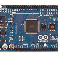
A000047 Arduino, A000047 Datasheet - Page 301
A000047
Manufacturer Part Number
A000047
Description
MCU, MPU & DSP Development Tools Mega2560
Manufacturer
Arduino
Series
-r
Type
MCUr
Specifications of A000047
Processor To Be Evaluated
ATmega2560
Interface Type
USB, I2C, SPI
Dimensions
4 in x 2.1 in
Operating Supply Voltage
5 V
Contents
Board
Lead Free Status / RoHS Status
Lead free / RoHS Compliant
For Use With/related Products
ATmega2560


26.7
26.8
26.9
26.9.1
2549M–AVR–09/10
Using the JTAG Programming Capabilities
Bibliography
On-chip Debug Related Register in I/O Memory
OCDR – On-chip Debug Register
Programming of AVR parts via JTAG is performed via the 4-pin JTAG port, TCK, TMS, TDI, and
TDO. These are the only pins that need to be controlled/observed to perform JTAG program-
ming (in addition to power pins). It is not required to apply 12V externally. The JTAGEN Fuse
must be programmed and the JTD bit in the MCUCR Register must be cleared to enable the
JTAG Test Access Port.
The JTAG programming capability supports:
•
•
•
•
The Lock bit security is exactly as in parallel programming mode. If the Lock bits LB1 or LB2 are
programmed, the OCDEN Fuse cannot be programmed unless first doing a chip erase. This is a
security feature that ensures no back-door exists for reading out the content of a secured
device.
The details on programming through the JTAG interface and programming specific JTAG
instructions are given in the section
For more information about general Boundary-scan, the following literature can be consulted:
•
•
The OCDR Register provides a communication channel from the running program in the micro-
controller to the debugger. The CPU can transfer a byte to the debugger by writing to this
location. At the same time, an internal flag; I/O Debug Register Dirty – IDRD – is set to indicate
to the debugger that the register has been written. When the CPU reads the OCDR Register the
7 LSB will be from the OCDR Register, while the MSB is the IDRD bit. The debugger clears the
IDRD bit when it has read the information.
In some AVR devices, this register is shared with a standard I/O location. In this case, the OCDR
Register can only be accessed if the OCDEN Fuse is programmed, and the debugger enables
access to the OCDR Register. In all other cases, the standard I/O location is accessed.
Refer to the debugger documentation for further information on how to use this register.
Bit
0x31 (0x51)
Read/Write
Initial Value
Flash programming and verifying.
EEPROM programming and verifying.
Fuse programming and verifying.
Lock bit programming and verifying.
IEEE: IEEE Std. 1149.1-1990. IEEE Standard Test Access Port and Boundary-scan
Architecture, IEEE, 1993.
Colin Maunder: The Board Designers Guide to Testable Logic Circuits, Addison-Wesley,
1992.
MSB/IDRD
R/W
7
0
R/W
6
0
ATmega640/1280/1281/2560/2561
“Programming via the JTAG Interface” on page
R/W
5
0
R/W
4
0
R/W
3
0
R/W
2
0
R/W
1
0
LSB
R/W
0
0
354.
OCDR
301
Related parts for A000047
Image
Part Number
Description
Manufacturer
Datasheet
Request
R

Part Number:
Description:
Daughter Cards & OEM Boards ARDUINO UNO PROTO PCB REV 3
Manufacturer:
Arduino
Part Number:
Description:
Daughter Cards & OEM Boards ARDUINO SHIELD PROTO KIT REV 3
Manufacturer:
Arduino
Part Number:
Description:
Daughter Cards & OEM Boards ARDUINO MEGA PROTO KIT REV 3
Manufacturer:
Arduino
Part Number:
Description:
Daughter Cards & OEM Boards ARDUINO MEGA PROTO PCB REV 3
Manufacturer:
Arduino
Part Number:
Description:
Development Boards & Kits - AVR ARDUINO STARTER KIT W/ UNO REV3
Manufacturer:
Arduino
Part Number:
Description:
RF Development Tools ARDUINO SHIELD WIRELESS PROTO
Manufacturer:
Arduino
Datasheet:
Part Number:
Description:
RF Development Tools ARDUINO SHIELD WIRELESS WITH SD
Manufacturer:
Arduino
Datasheet:

Part Number:
Description:
Development Software Getting started w/Arduino
Manufacturer:
Arduino

Part Number:
Description:
Ethernet Modules & Development Tools Ethernet Shield for Arduino
Manufacturer:
Arduino

Part Number:
Description:
MCU, MPU & DSP Development Tools LilyPad Arduino Main Board
Manufacturer:
Arduino

Part Number:
Description:
ARDUINO NANO Board
Manufacturer:
Arduino
Datasheet:
Part Number:
Description:
Ethernet Modules & Development Tools ETHERNET SHEILD PoE FOR ARDUINO
Manufacturer:
Arduino
Datasheet:

Part Number:
Description:
ATMEGA328 MCU IC W/ Arduino UNO Bootloader
Manufacturer:
Arduino
Datasheet:
Part Number:
Description:
Memory Cards MICRO SD CARD 1GB WITH SD ADAPTER
Manufacturer:
Arduino