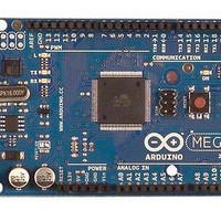
A000047 Arduino, A000047 Datasheet - Page 27
A000047
Manufacturer Part Number
A000047
Description
MCU, MPU & DSP Development Tools Mega2560
Manufacturer
Arduino
Series
-r
Type
MCUr
Specifications of A000047
Processor To Be Evaluated
ATmega2560
Interface Type
USB, I2C, SPI
Dimensions
4 in x 2.1 in
Operating Supply Voltage
5 V
Contents
Board
Lead Free Status / RoHS Status
Lead free / RoHS Compliant
For Use With/related Products
ATmega2560


7.4
7.4.1
2549M–AVR–09/10
I/O Memory
General Purpose I/O Registers
The I/O space definition of the ATmega640/1280/1281/2560/2561 is shown in
mary” on page
All ATmega640/1280/1281/2560/2561 I/Os and peripherals are placed in the I/O space. All I/O
locations may be accessed by the LD/LDS/LDD and ST/STS/STD instructions, transferring data
between the 32 general purpose working registers and the I/O space. I/O Registers within the
address range 0x00 - 0x1F are directly bit-accessible using the SBI and CBI instructions. In
these registers, the value of single bits can be checked by using the SBIS and SBIC instructions.
Refer to the instruction set section for more details. When using the I/O specific commands IN
and OUT, the I/O addresses 0x00 - 0x3F must be used. When addressing I/O Registers as data
space using LD and ST instructions, 0x20 must be added to these addresses. The
ATmega640/1280/1281/2560/2561 is a complex microcontroller with more peripheral units than
can be supported within the 64 location reserved in Opcode for the IN and OUT instructions. For
the Extended I/O space from 0x60 - 0x1FF in SRAM, only the ST/STS/STD and LD/LDS/LDD
instructions can be used.
For compatibility with future devices, reserved bits should be written to zero if accessed.
Reserved I/O memory addresses should never be written.
Some of the Status Flags are cleared by writing a logical one to them. Note that, unlike most
other AVRs, the CBI and SBI instructions will only operate on the specified bit, and can therefore
be used on registers containing such Status Flags. The CBI and SBI instructions work with reg-
isters 0x00 to 0x1F only.
The I/O and peripherals control registers are explained in later sections.
The ATmega640/1280/1281/2560/2561 contains three General Purpose I/O Registers. These
registers can be used for storing any information, and they are particularly useful for storing
global variables and Status Flags. General Purpose I/O Registers within the address range 0x00
- 0x1F are directly bit-accessible using the SBI, CBI, SBIS, and SBIC instructions. See
Description” on page
410.
35.
ATmega640/1280/1281/2560/2561
“Register Sum-
“Register
27
Related parts for A000047
Image
Part Number
Description
Manufacturer
Datasheet
Request
R

Part Number:
Description:
Daughter Cards & OEM Boards ARDUINO UNO PROTO PCB REV 3
Manufacturer:
Arduino
Part Number:
Description:
Daughter Cards & OEM Boards ARDUINO SHIELD PROTO KIT REV 3
Manufacturer:
Arduino
Part Number:
Description:
Daughter Cards & OEM Boards ARDUINO MEGA PROTO KIT REV 3
Manufacturer:
Arduino
Part Number:
Description:
Daughter Cards & OEM Boards ARDUINO MEGA PROTO PCB REV 3
Manufacturer:
Arduino
Part Number:
Description:
Development Boards & Kits - AVR ARDUINO STARTER KIT W/ UNO REV3
Manufacturer:
Arduino
Part Number:
Description:
RF Development Tools ARDUINO SHIELD WIRELESS PROTO
Manufacturer:
Arduino
Datasheet:
Part Number:
Description:
RF Development Tools ARDUINO SHIELD WIRELESS WITH SD
Manufacturer:
Arduino
Datasheet:

Part Number:
Description:
Development Software Getting started w/Arduino
Manufacturer:
Arduino

Part Number:
Description:
Ethernet Modules & Development Tools Ethernet Shield for Arduino
Manufacturer:
Arduino

Part Number:
Description:
MCU, MPU & DSP Development Tools LilyPad Arduino Main Board
Manufacturer:
Arduino

Part Number:
Description:
ARDUINO NANO Board
Manufacturer:
Arduino
Datasheet:
Part Number:
Description:
Ethernet Modules & Development Tools ETHERNET SHEILD PoE FOR ARDUINO
Manufacturer:
Arduino
Datasheet:

Part Number:
Description:
ATMEGA328 MCU IC W/ Arduino UNO Bootloader
Manufacturer:
Arduino
Datasheet:
Part Number:
Description:
Memory Cards MICRO SD CARD 1GB WITH SD ADAPTER
Manufacturer:
Arduino