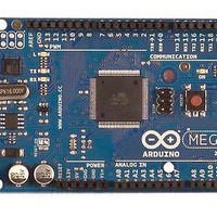
A000047 Arduino, A000047 Datasheet - Page 23
A000047
Manufacturer Part Number
A000047
Description
MCU, MPU & DSP Development Tools Mega2560
Manufacturer
Arduino
Series
-r
Type
MCUr
Specifications of A000047
Processor To Be Evaluated
ATmega2560
Interface Type
USB, I2C, SPI
Dimensions
4 in x 2.1 in
Operating Supply Voltage
5 V
Contents
Board
Lead Free Status / RoHS Status
Lead free / RoHS Compliant
For Use With/related Products
ATmega2560


7.2.1
7.3
2549M–AVR–09/10
EEPROM Data Memory
Data Memory Access Times
Figure 7-2.
This section describes the general access timing concepts for internal memory access. The
internal data SRAM access is performed in two clk
Figure 7-3.
The ATmega640/1280/1281/2560/2561 contains 4 Kbytes of data EEPROM memory. It is orga-
nized as a separate data space, in which single bytes can be read and written. The EEPROM
has an endurance of at least 100,000 write/erase cycles. The access between the EEPROM and
the CPU is described in the following, specifying the EEPROM Address Registers, the EEPROM
Data Register, and the EEPROM Control Register.
For a detailed description of SPI, JTAG and Parallel data downloading to the EEPROM, see
“Serial Downloading” on page
“Programming the EEPROM” on page 343
Address (HEX)
60 - 1FF
20 - 5F
0 - 1F
FFFF
Address
21FF
2200
200
clk
Data Memory Map
On-chip Data SRAM Access Cycles
Data
Data
WR
CPU
RD
Compute Address
349,
ATmega640/1280/1281/2560/2561
T1
Memory Access Instruction
416 External I/O Registers
“Programming via the JTAG Interface” on page
64 I/O Registers
External SRAM
Internal SRAM
32 Registers
(0 - 64K x 8)
respectively.
(8192 x 8)
Address valid
CPU
T2
cycles as described in
Next Instruction
T3
Figure
7-3.
354, and
23
Related parts for A000047
Image
Part Number
Description
Manufacturer
Datasheet
Request
R

Part Number:
Description:
Daughter Cards & OEM Boards ARDUINO UNO PROTO PCB REV 3
Manufacturer:
Arduino
Part Number:
Description:
Daughter Cards & OEM Boards ARDUINO SHIELD PROTO KIT REV 3
Manufacturer:
Arduino
Part Number:
Description:
Daughter Cards & OEM Boards ARDUINO MEGA PROTO KIT REV 3
Manufacturer:
Arduino
Part Number:
Description:
Daughter Cards & OEM Boards ARDUINO MEGA PROTO PCB REV 3
Manufacturer:
Arduino
Part Number:
Description:
Development Boards & Kits - AVR ARDUINO STARTER KIT W/ UNO REV3
Manufacturer:
Arduino
Part Number:
Description:
RF Development Tools ARDUINO SHIELD WIRELESS PROTO
Manufacturer:
Arduino
Datasheet:
Part Number:
Description:
RF Development Tools ARDUINO SHIELD WIRELESS WITH SD
Manufacturer:
Arduino
Datasheet:

Part Number:
Description:
Development Software Getting started w/Arduino
Manufacturer:
Arduino

Part Number:
Description:
Ethernet Modules & Development Tools Ethernet Shield for Arduino
Manufacturer:
Arduino

Part Number:
Description:
MCU, MPU & DSP Development Tools LilyPad Arduino Main Board
Manufacturer:
Arduino

Part Number:
Description:
ARDUINO NANO Board
Manufacturer:
Arduino
Datasheet:
Part Number:
Description:
Ethernet Modules & Development Tools ETHERNET SHEILD PoE FOR ARDUINO
Manufacturer:
Arduino
Datasheet:

Part Number:
Description:
ATMEGA328 MCU IC W/ Arduino UNO Bootloader
Manufacturer:
Arduino
Datasheet:
Part Number:
Description:
Memory Cards MICRO SD CARD 1GB WITH SD ADAPTER
Manufacturer:
Arduino