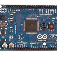
A000047 Arduino, A000047 Datasheet - Page 147
A000047
Manufacturer Part Number
A000047
Description
MCU, MPU & DSP Development Tools Mega2560
Manufacturer
Arduino
Series
-r
Type
MCUr
Specifications of A000047
Processor To Be Evaluated
ATmega2560
Interface Type
USB, I2C, SPI
Dimensions
4 in x 2.1 in
Operating Supply Voltage
5 V
Contents
Board
Lead Free Status / RoHS Status
Lead free / RoHS Compliant
For Use With/related Products
ATmega2560


16.8
16.8.1
2549M–AVR–09/10
Compare Match Output Unit
Compare Output Mode and Waveform Generation
The Compare Output mode (COMnx1:0) bits have two functions. The Waveform Generator uses
the COMnx1:0 bits for defining the Output Compare (OCnx) state at the next compare match.
Secondly the COMnx1:0 bits control the OCnx pin output source.
schematic of the logic affected by the COMnx1:0 bit setting. The I/O Registers, I/O bits, and I/O
pins in the figure are shown in bold. Only the parts of the general I/O Port Control Registers
(DDR and PORT) that are affected by the COMnx1:0 bits are shown. When referring to the
OCnx state, the reference is for the internal OCnx Register, not the OCnx pin. If a system reset
occur, the OCnx Register is reset to “0”.
Figure 16-5. Compare Match Output Unit, Schematic
The general I/O port function is overridden by the Output Compare (OCnx) from the Waveform
Generator if either of the COMnx1:0 bits are set. However, the OCnx pin direction (input or out-
put) is still controlled by the Data Direction Register (DDR) for the port pin. The Data Direction
Register bit for the OCnx pin (DDR_OCnx) must be set as output before the OCnx value is visi-
ble on the pin. The port override function is generally independent of the Waveform Generation
mode, but there are some exceptions. Refer to
and
The design of the Output Compare pin logic allows initialization of the OCnx state before the out-
put is enabled. Note that some COMnx1:0 bit settings are reserved for certain modes of
operation.
The COMnx1:0 bits have no effect on the Input Capture unit.
The Waveform Generator uses the COMnx1:0 bits differently in normal, CTC, and PWM modes.
For all modes, setting the COMnx1:0 = 0 tells the Waveform Generator that no action on the
OCnx Register is to be performed on the next compare match. For compare output actions in the
Table 16-5 on page 160
COMnx1
COMnx0
FOCnx
clk
I/O
See “Register Description” on page 158.
Waveform
Generator
for details.
ATmega640/1280/1281/2560/2561
D
D
D
PORT
DDR
OCnx
Table 16-3 on page
Q
Q
Q
1
0
Figure 16-5
159,
Table 16-4 on page 159
shows a simplified
OCnx
Pin
147
Related parts for A000047
Image
Part Number
Description
Manufacturer
Datasheet
Request
R

Part Number:
Description:
Daughter Cards & OEM Boards ARDUINO UNO PROTO PCB REV 3
Manufacturer:
Arduino
Part Number:
Description:
Daughter Cards & OEM Boards ARDUINO SHIELD PROTO KIT REV 3
Manufacturer:
Arduino
Part Number:
Description:
Daughter Cards & OEM Boards ARDUINO MEGA PROTO KIT REV 3
Manufacturer:
Arduino
Part Number:
Description:
Daughter Cards & OEM Boards ARDUINO MEGA PROTO PCB REV 3
Manufacturer:
Arduino
Part Number:
Description:
Development Boards & Kits - AVR ARDUINO STARTER KIT W/ UNO REV3
Manufacturer:
Arduino
Part Number:
Description:
RF Development Tools ARDUINO SHIELD WIRELESS PROTO
Manufacturer:
Arduino
Datasheet:
Part Number:
Description:
RF Development Tools ARDUINO SHIELD WIRELESS WITH SD
Manufacturer:
Arduino
Datasheet:

Part Number:
Description:
Development Software Getting started w/Arduino
Manufacturer:
Arduino

Part Number:
Description:
Ethernet Modules & Development Tools Ethernet Shield for Arduino
Manufacturer:
Arduino

Part Number:
Description:
MCU, MPU & DSP Development Tools LilyPad Arduino Main Board
Manufacturer:
Arduino

Part Number:
Description:
ARDUINO NANO Board
Manufacturer:
Arduino
Datasheet:
Part Number:
Description:
Ethernet Modules & Development Tools ETHERNET SHEILD PoE FOR ARDUINO
Manufacturer:
Arduino
Datasheet:

Part Number:
Description:
ATMEGA328 MCU IC W/ Arduino UNO Bootloader
Manufacturer:
Arduino
Datasheet:
Part Number:
Description:
Memory Cards MICRO SD CARD 1GB WITH SD ADAPTER
Manufacturer:
Arduino