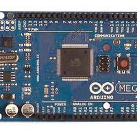
A000047 Arduino, A000047 Datasheet - Page 156
A000047
Manufacturer Part Number
A000047
Description
MCU, MPU & DSP Development Tools Mega2560
Manufacturer
Arduino
Series
-r
Type
MCUr
Specifications of A000047
Processor To Be Evaluated
ATmega2560
Interface Type
USB, I2C, SPI
Dimensions
4 in x 2.1 in
Operating Supply Voltage
5 V
Contents
Board
Lead Free Status / RoHS Status
Lead free / RoHS Compliant
For Use With/related Products
ATmega2560


16.10 Timer/Counter Timing Diagrams
2549M–AVR–09/10
The extreme values for the OCRnx Register represents special cases when generating a PWM
waveform output in the phase correct PWM mode. If the OCRnx is set equal to BOTTOM the
output will be continuously low and if set equal to TOP the output will be set to high for non-
inverted PWM mode. For inverted PWM the output will have the opposite logic values. If OCR1A
is used to define the TOP value (WGM13:0 = 9) and COM1A1:0 = 1, the OC1A output will toggle
with a 50% duty cycle.
The Timer/Counter is a synchronous design and the timer clock (clk
clock enable signal in the following figures. The figures include information on when Interrupt
Flags are set, and when the OCRnx Register is updated with the OCRnx buffer value (only for
modes utilizing double buffering).
Figure 16-10. Timer/Counter Timing Diagram, Setting of OCFnx, no Prescaling
Figure 16-11
Figure 16-11. Timer/Counter Timing Diagram, Setting of OCFnx, with Prescaler (f
TCNTn
OCRnx
OCFnx
TCNTn
OCRnx
(clk
OCFnx
(clk
clk
clk
clk
clk
I/O
I/O
I/O
Tn
I/O
Tn
/1)
/8)
shows the same timing data, but with the prescaler enabled.
OCRnx - 1
OCRnx - 1
ATmega640/1280/1281/2560/2561
Figure 16-10
OCRnx
OCRnx
OCRnx Value
OCRnx Value
shows a timing diagram for the setting of OCFnx.
OCRnx + 1
OCRnx + 1
Tn
) is therefore shown as a
OCRnx + 2
OCRnx + 2
clk_I/O
/8)
156
Related parts for A000047
Image
Part Number
Description
Manufacturer
Datasheet
Request
R

Part Number:
Description:
Daughter Cards & OEM Boards ARDUINO UNO PROTO PCB REV 3
Manufacturer:
Arduino
Part Number:
Description:
Daughter Cards & OEM Boards ARDUINO SHIELD PROTO KIT REV 3
Manufacturer:
Arduino
Part Number:
Description:
Daughter Cards & OEM Boards ARDUINO MEGA PROTO KIT REV 3
Manufacturer:
Arduino
Part Number:
Description:
Daughter Cards & OEM Boards ARDUINO MEGA PROTO PCB REV 3
Manufacturer:
Arduino
Part Number:
Description:
Development Boards & Kits - AVR ARDUINO STARTER KIT W/ UNO REV3
Manufacturer:
Arduino
Part Number:
Description:
RF Development Tools ARDUINO SHIELD WIRELESS PROTO
Manufacturer:
Arduino
Datasheet:
Part Number:
Description:
RF Development Tools ARDUINO SHIELD WIRELESS WITH SD
Manufacturer:
Arduino
Datasheet:

Part Number:
Description:
Development Software Getting started w/Arduino
Manufacturer:
Arduino

Part Number:
Description:
Ethernet Modules & Development Tools Ethernet Shield for Arduino
Manufacturer:
Arduino

Part Number:
Description:
MCU, MPU & DSP Development Tools LilyPad Arduino Main Board
Manufacturer:
Arduino

Part Number:
Description:
ARDUINO NANO Board
Manufacturer:
Arduino
Datasheet:
Part Number:
Description:
Ethernet Modules & Development Tools ETHERNET SHEILD PoE FOR ARDUINO
Manufacturer:
Arduino
Datasheet:

Part Number:
Description:
ATMEGA328 MCU IC W/ Arduino UNO Bootloader
Manufacturer:
Arduino
Datasheet:
Part Number:
Description:
Memory Cards MICRO SD CARD 1GB WITH SD ADAPTER
Manufacturer:
Arduino