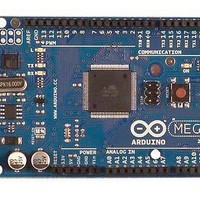
A000047 Arduino, A000047 Datasheet - Page 337
A000047
Manufacturer Part Number
A000047
Description
MCU, MPU & DSP Development Tools Mega2560
Manufacturer
Arduino
Series
-r
Type
MCUr
Specifications of A000047
Processor To Be Evaluated
ATmega2560
Interface Type
USB, I2C, SPI
Dimensions
4 in x 2.1 in
Operating Supply Voltage
5 V
Contents
Board
Lead Free Status / RoHS Status
Lead free / RoHS Compliant
For Use With/related Products
ATmega2560


2549M–AVR–09/10
Table 29-4.
Notes:
Table 29-5.
Notes:
The status of the Fuse bits is not affected by Chip Erase. Note that the Fuse bits are locked if
Lock bit1 (LB1) is programmed. Program the Fuse bits before programming the Lock bits.
Fuse High Byte
OCDEN
JTAGEN
SPIEN
WDTON
EESAVE
BOOTSZ1
BOOTSZ0
BOOTRST
Fuse Low Byte
CKDIV8
CKOUT
SUT1
SUT0
CKSEL3
CKSEL2
CKSEL1
CKSEL0
(1)
1. The SPIEN Fuse is not accessible in serial programming mode.
2. The default value of BOOTSZ1:0 results in maximum Boot Size. See
3. See
4. Never ship a product with the OCDEN Fuse programmed regardless of the setting of Lock bits
1. The default value of SUT1:0 results in maximum start-up time for the default clock source. See
2. The default setting of CKSEL3:0 results in internal RC Oscillator @ 8 MHz. See
3. The CKOUT Fuse allow the system clock to be output on PORTE7. See
4. See
(3)
(4)
(4)
(3)
for details.
and JTAGEN Fuse. A programmed OCDEN Fuse enables some parts of the clock system to
be running in all sleep modes. This may increase the power consumption.
“System and Reset Characteristics” on page 372
page 41
on page 49
Fuse High Byte
Fuse Low Byte
“WDTCSR – Watchdog Timer Control Register” on page 67
“System Clock Prescaler” on page 49
for details.
Bit No
for details.
7
6
5
4
3
2
1
0
Bit No
7
6
5
4
3
2
1
0
Description
Enable OCD
Enable JTAG
Enable Serial Program and Data
Downloading
Watchdog Timer always on
EEPROM memory is preserved
through the Chip Erase
Select Boot Size (see
page 339
Select Boot Size (see
page 339
Select Reset Vector
ATmega640/1280/1281/2560/2561
Description
Divide clock by 8
Clock output
Select start-up time
Select start-up time
Select Clock source
Select Clock source
Select Clock source
Select Clock source
for details)
for details)
for details.
Table 29-9 on
Table 29-9 on
for details.
Default Value
1 (unprogrammed, OCD
disabled)
0 (programmed, JTAG enabled)
0 (programmed, SPI prog.
enabled)
1 (unprogrammed)
1 (unprogrammed, EEPROM
not preserved)
0 (programmed)
0 (programmed)
1 (unprogrammed)
1 (unprogrammed)
Default Value
0 (programmed)
1 (unprogrammed)
0 (programmed)
0 (programmed)
0 (programmed)
1 (unprogrammed)
0 (programmed)
for details.
Table 28-7 on page 328
“Clock Output Buffer”
(2)
(2)
(1)
(2)
(2)
(2)
Table 9-1 on
(1)
(2)
337
Related parts for A000047
Image
Part Number
Description
Manufacturer
Datasheet
Request
R

Part Number:
Description:
Daughter Cards & OEM Boards ARDUINO UNO PROTO PCB REV 3
Manufacturer:
Arduino
Part Number:
Description:
Daughter Cards & OEM Boards ARDUINO SHIELD PROTO KIT REV 3
Manufacturer:
Arduino
Part Number:
Description:
Daughter Cards & OEM Boards ARDUINO MEGA PROTO KIT REV 3
Manufacturer:
Arduino
Part Number:
Description:
Daughter Cards & OEM Boards ARDUINO MEGA PROTO PCB REV 3
Manufacturer:
Arduino
Part Number:
Description:
Development Boards & Kits - AVR ARDUINO STARTER KIT W/ UNO REV3
Manufacturer:
Arduino
Part Number:
Description:
RF Development Tools ARDUINO SHIELD WIRELESS PROTO
Manufacturer:
Arduino
Datasheet:
Part Number:
Description:
RF Development Tools ARDUINO SHIELD WIRELESS WITH SD
Manufacturer:
Arduino
Datasheet:

Part Number:
Description:
Development Software Getting started w/Arduino
Manufacturer:
Arduino

Part Number:
Description:
Ethernet Modules & Development Tools Ethernet Shield for Arduino
Manufacturer:
Arduino

Part Number:
Description:
MCU, MPU & DSP Development Tools LilyPad Arduino Main Board
Manufacturer:
Arduino

Part Number:
Description:
ARDUINO NANO Board
Manufacturer:
Arduino
Datasheet:
Part Number:
Description:
Ethernet Modules & Development Tools ETHERNET SHEILD PoE FOR ARDUINO
Manufacturer:
Arduino
Datasheet:

Part Number:
Description:
ATMEGA328 MCU IC W/ Arduino UNO Bootloader
Manufacturer:
Arduino
Datasheet:
Part Number:
Description:
Memory Cards MICRO SD CARD 1GB WITH SD ADAPTER
Manufacturer:
Arduino