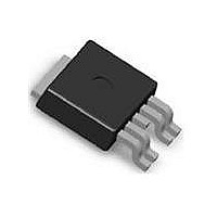
FDD8426H Fairchild Semiconductor, FDD8426H Datasheet

FDD8426H
Specifications of FDD8426H
Related parts for FDD8426H
FDD8426H Summary of contents
Page 1
... Thermal Resistance, Junction to Case, Single Operation for Q2 θJC Package Marking and Ordering Information Device Marking Device FDD8426H FDD8426H ©2009 Fairchild Semiconductor Corporation FDD8426H Rev.C ® MOSFET General Description These dual N and P-Channel enhancement mode Power MOSFETs are produced using Fairchild Semiconductor’ ...
Page 2
... Fall Time f Q Total Gate Charge g(TOT) Q Total Gate Charge g(TOT) Q Gate to Source Charge gs Q Gate to Drain “Miller” Charge gd ©2009 Fairchild Semiconductor Corporation FDD8426H Rev 25°C unless otherwise noted J Test Conditions = 250 µ -250 µ 250 µA, referenced to 25 °C ...
Page 3
... Q Reverse Recovery Charge rr Notes determined with the device mounted on a 1in θJA by the user's board design Pulse Test: Pulse Width < 300 µs, Duty cycle < 2.0%. 3. Starting °C, N-ch mH ©2009 Fairchild Semiconductor Corporation FDD8426H Rev 25°C unless otherwise noted J Test Conditions - di/dt = 100 A/µs ...
Page 4
... PULSE DURATION = 80 s DUTY CYCLE = 0.5% MAX 150 GATE TO SOURCE VOLTAGE (V) GS Figure 5. Transfer Characteristics ©2009 Fairchild Semiconductor Corporation FDD8426H Rev 25°C unless otherwise noted J 2.5 2.0 1.5 1.0 µ s 0.5 1.5 2.0 300 200 100 50 75 100 125 150 ...
Page 5
... THIS AREA IS LIMITED BY r DS(on) 1 SINGLE PULSE T = MAX RATED 1.4 C/W θ 0.1 0 DRAIN to SOURCE VOLTAGE (V) DS Figure 11. Forward Bias Safe Operating Area ©2009 Fairchild Semiconductor Corporation FDD8426H Rev 25°C unless otherwise noted J 5000 = 1000 100 150 100 1000 100 us ...
Page 6
... DUTY CYCLE-DESCENDING ORDER 0.5 0.2 0.1 0.1 0.05 0.02 0.01 0.01 0.001 SINGLE PULSE R ( Note 1b 0.0001 - Figure 14. ©2009 Fairchild Semiconductor Corporation FDD8426H Rev 25°C unless otherwise noted 1.4 C RECTANGULAR PULSE DURATION (sec C/W θ RECTANGULAR PULSE DURATION (sec) Junction-to-Ambient Transient Thermal Response Curve ...
Page 7
... PULSE DURATION = 80 s DUTY CYCLE = 0.5% MAX 150 1.5 2.0 2.5 3 GATE TO SOURCE VOLTAGE (V) GS Figure 19. Transfer Characteristics ©2009 Fairchild Semiconductor Corporation FDD8426H Rev °C unless otherwise noted J µ Figure 16. Normalized on-Resistance vs Drain 50 75 100 125 150 0 - 0.01 3.5 4.0 4 ...
Page 8
... LIMITED BY r ds(on) SINGLE PULSE MAX RATED 1.4 C/W θ 0.1 0 DRAIN to SOURCE VOLTAGE (V) DS Figure 25. Forward Bias Safe Operating Area ©2009 Fairchild Semiconductor Corporation FDD8426H Rev 25°C unless otherwise noted J 5000 1000 100 100 500 Figure 24. Maximum Continuous Drain 1000 ...
Page 9
... DUTY CYCLE-DESCENDING ORDER 0.5 0.1 0.2 0.1 0.05 0.02 0.01 0.01 0.001 SINGLE PULSE R θ ( Note 1b 0.0001 - Figure 28. Junction-to-Ambient Transient Thermal Response Curve ©2009 Fairchild Semiconductor Corporation FDD8426H Rev °C unless otherwise noted RECTANGULAR PULSE DURATION (sec C RECTANGULAR PULSE DURATION (sec ...
Page 10
... Dimensional Outline and Pad Layout ©2009 Fairchild Semiconductor Corporation FDD8426H Rev.C 10 www.fairchildsemi.com ...
Page 11
... Datasheet Identification Product Status Advance Information Formative / In Design Preliminary First Production No Identification Needed Full Production Obsolete Not In Production ©2009 Fairchild Semiconductor Corporation FDD8426H Rev.C FPS™ PowerTrench F-PFS™ PowerXS™ ® FRFET Programmable Active Droop™ SM ® Global Power Resource QFET Green FPS™ ...


