EM250-DEV Ember, EM250-DEV Datasheet - Page 99
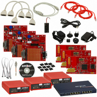
EM250-DEV
Manufacturer Part Number
EM250-DEV
Description
KIT DEV FOR EM250
Manufacturer
Ember
Series
InSightr
Type
802.15.4/Zigbeer
Specifications of EM250-DEV
Frequency
2.4GHz
For Use With/related Products
EM250
Lead Free Status / RoHS Status
Contains lead / RoHS non-compliant
Other names
636-1002


ADC_CFG [0x4902]
ADC_RATE
ADC_SEL
ADC_DITH
ADC_EN
0-R
0-R
15
0
0
7
Table 36 lists the specifications for the ADC.
Parameter
Conversion time
VREF
VREF output current
VREF load capacitance
Minimum input voltage
Maximum input voltage
Single-ended signal range
Differential signal range
Common mode range
Input referred ADC offset
The signal-ended ADC measurements are limited in their range and only guaranteed for accuracy in the range
0 to VREF. The nature of the ADC's internal design allows for measurements outside of this range, but such
measurements are not guaranteed and instead act as a factor of safety. Maximum input voltage, VDD, can be
treated as the failure point. Measurement is not guaranteed at this level, and damage is possible above this
level. The maximum input voltage is of more interest to the differential sampling where a differential meas-
urement might be small, but a common mode can push the actual input voltage on one of the signals towards
VDD.
5.5.1
0-RW
0-R
14
0
6
[14:12]
[11:8]
[1]
[0]
Registers
ADC_RATE
ADC conversion rate selection. Refer to Table 33 for details.
ADC input selection. Refer to Table 34 for details.
Set this bit to disable dither.
Set this bit to enable the ADC.
0-RW
0-R
13
0
5
0-RW
0-R
12
0
4
Table 36. ADC Specifications
0-RW
0-R
11
0
3
0
0
0
- 10
Min.
32
- VREF
0-RW
0-R
10
0
2
ADC_SEL
Typ.
1.2
ADC_DITH
0-RW
0-RW
9
1
Max.
4096
1
10
VDD
VREF
+ VREF
VREF
10
120-0082-000I
EM250
mV
Unit
µs
V
mA
nF
V
V
V
V
V
ADC_EN
0-RW
0-RW
8
0
99
Related parts for EM250-DEV
Image
Part Number
Description
Manufacturer
Datasheet
Request
R

Part Number:
Description:
IC ZIGBEE SYSTEM-ON-CHIP 48-QFN
Manufacturer:
Ember
Datasheet:

Part Number:
Description:
EM250 RCM BOARD
Manufacturer:
Ember
Datasheet:

Part Number:
Description:
EM250 BREAKOUT BOARD
Manufacturer:
Ember
Datasheet:

Part Number:
Description:
KIT JUMP START FOR EM250
Manufacturer:
Ember
Datasheet:

Part Number:
Description:
KIT EVAL EM250 RF TEST
Manufacturer:
Ember
Datasheet:

Part Number:
Description:
KIT DEV EMBER ZIGBEE W/PCWH
Manufacturer:
Custom Computer Services Inc (CCS)

Part Number:
Description:
PROGRAMMER USB FLASH EM250/260
Manufacturer:
Ember
Datasheet:

Part Number:
Description:
IC ZIGBEE SYSTEM-ON-CHIP 40-QFN
Manufacturer:
Ember
Datasheet:
Part Number:
Description:
IC RF TXRX ZIGBEE 128KB 48QFN
Manufacturer:
Ember
Datasheet:
Part Number:
Description:
IC RF TXRX ZIGBEE 192KB 48QFN
Manufacturer:
Ember
Datasheet:

Part Number:
Description:
INSIGHT ADAPTER FOR EM2XX
Manufacturer:
Ember
Datasheet:

Part Number:
Description:
IAR EWARM LICENCE FOR EM35X
Manufacturer:
Ember
Datasheet:

Part Number:
Description:
INSIGHT ADAPTER 3 FOR EM35X
Manufacturer:
Ember
Datasheet:

Part Number:
Description:
EM35X BREAKOUT BOARD
Manufacturer:
Ember
Datasheet:

Part Number:
Description:
EM260 RCM BOARD
Manufacturer:
Ember
Datasheet: