EM250-DEV Ember, EM250-DEV Datasheet - Page 42
EM250-DEV
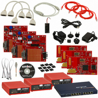
Manufacturer Part Number
EM250-DEV
Description
KIT DEV FOR EM250
Manufacturer
Ember
Series
InSightr
Type
802.15.4/Zigbeer
Specifications of EM250-DEV
Frequency
2.4GHz
For Use With/related Products
EM250
Lead Free Status / RoHS Status
Contains lead / RoHS non-compliant
Other names
636-1002


EM250
42
120-0082-000I
hardware generates the
til the RX FIFO is drained. Once the DMA marks a RX error, there are two conditions that will clear the error
indication: setting the appropriate
priate DMA buffer after it has unloaded.
Interrupts are generated on the following events:
To generate interrupts to the CPU, the interrupt masks in the
abled.
5.2.2
The SPI mode of the SC1 is master mode only. It has a fixed word length of 8 bits. The SC1 SPI controller is en-
abled with
The SPI mode has the following features:
The following signals can be made available on the GPIO pins:
The SC1 SPI module obtains its reference clock from a programmable clock generator. Clock rates are set by a
clock division ratio from the 24MHz clock:
EXP is written to the
values is 0 to 15, the fastest data rate is 12Mbps and the slowest rate is 22.9bps.
The SC1 SPI master supports various frame formats depending upon the clock polarity (
phase (
SC_SPIPHA
Note: Switching the SPI configuration from
Transmit FIFO empty and last character shifted out (0 to 1 transition of
Transmit FIFO changed from full to not full (0 to 1 transition of
Receive FIFO changed from empty to not empty (0 to 1 transition of
Transmit DMA buffer A/B complete (1 to 0 transition of
Receive DMA buffer A/B complete (1 to 0 transition of
Character received with Parity error
Character received with Frame error
Received and lost character while receive FIFO was full (Receive overrun error)
Full duplex operation
Programmable clock frequency (12MHz max.)
Programmable clock polarity and clock phase
Selectable data shift direction (either LSB or MSB first)
MO (master out)
MI (master in)
MCLK (serial clock)
rate = 24MHz / ( 2 * (LIN + 1) * 2
SC_SPIPHA
SPI Master Mode
SC1_MODE=0
before the first intended byte.
SC1_MODE
, and
SC_SPIORD
), and direction of data (
SC1_RATEEXP
and reinitializing the SPI will cause an extra byte (
set to 2 and register bit
INT_SCRXOVF
are defined within the
SC_TX/RXDMARST
register and LIN to the
EXP
interrupt, but the DMA register will not indicate the error condition un-
)
SC_SPIORD
SC_SPIPOL=1
SC_SPIMST
SC1_SPICFG
bit in the
) (see Table 21). The register bits
set in the
SC_RXACTA/B
SC1_RATELIN
to
SC_TXACTA/B
INT_SC1CFG
SC_SPIPOL=0
SC1_DMACTRL
register.
SC1_UARTTXFREE
SC1_SPICFG
0xFE
)
SC1_UARTRXVAL
register. Since the range for both
)
and
SC1_UARTTXIDLE
without subsequently setting
) to be transmitted immediately
register, or loading the appro-
INT_CFG
register.
)
SC_SPIPOL
SC_SPIPOL
)
registers must be en-
)
), clock
,
Related parts for EM250-DEV
Image
Part Number
Description
Manufacturer
Datasheet
Request
R

Part Number:
Description:
IC ZIGBEE SYSTEM-ON-CHIP 48-QFN
Manufacturer:
Ember
Datasheet:

Part Number:
Description:
EM250 RCM BOARD
Manufacturer:
Ember
Datasheet:

Part Number:
Description:
EM250 BREAKOUT BOARD
Manufacturer:
Ember
Datasheet:

Part Number:
Description:
KIT JUMP START FOR EM250
Manufacturer:
Ember
Datasheet:

Part Number:
Description:
KIT EVAL EM250 RF TEST
Manufacturer:
Ember
Datasheet:

Part Number:
Description:
KIT DEV EMBER ZIGBEE W/PCWH
Manufacturer:
Custom Computer Services Inc (CCS)

Part Number:
Description:
PROGRAMMER USB FLASH EM250/260
Manufacturer:
Ember
Datasheet:

Part Number:
Description:
IC ZIGBEE SYSTEM-ON-CHIP 40-QFN
Manufacturer:
Ember
Datasheet:
Part Number:
Description:
IC RF TXRX ZIGBEE 128KB 48QFN
Manufacturer:
Ember
Datasheet:
Part Number:
Description:
IC RF TXRX ZIGBEE 192KB 48QFN
Manufacturer:
Ember
Datasheet:

Part Number:
Description:
INSIGHT ADAPTER FOR EM2XX
Manufacturer:
Ember
Datasheet:

Part Number:
Description:
IAR EWARM LICENCE FOR EM35X
Manufacturer:
Ember
Datasheet:

Part Number:
Description:
INSIGHT ADAPTER 3 FOR EM35X
Manufacturer:
Ember
Datasheet:

Part Number:
Description:
EM35X BREAKOUT BOARD
Manufacturer:
Ember
Datasheet:

Part Number:
Description:
EM260 RCM BOARD
Manufacturer:
Ember
Datasheet: