EM250-DEV Ember, EM250-DEV Datasheet - Page 98
EM250-DEV
Manufacturer Part Number
EM250-DEV
Description
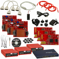
KIT DEV FOR EM250
Manufacturer
Ember
Series
InSightr
Type
802.15.4/Zigbeer
Specifications of EM250-DEV
Frequency
2.4GHz
For Use With/related Products
EM250
Lead Free Status / RoHS Status
Contains lead / RoHS non-compliant
Other names
636-1002


EM250
98
120-0082-000I
close to 1.2V as possible by the EmberZNet software, using the regulated supply (VDD) as reference. VREF is
able to source modest current (see Table 36) and is stable under capacitive loads. The ADC cannot accept an
external VREF input. For selecting alternate pin functions, refer to Table 17 and Table 18.
While the ADC Module supports both single-ended and differential inputs, the ADC input stage is differential.
Single-ended operation is provided by internally connecting one of the differential inputs to VREF/2 while fully
differential operation uses two external signals. The full-scale differential input range spans -VREF to +VREF
and the single-ended input range spans 0 to VREF.
Fully differential operation is recommended only when large common-mode signals are present. To correct
differential input for offset and gain, each side of the input should be sampled individually using single-ended
operation, so that they may be calibrated against VREF.
Sampling of internal connections VSS and VREF allow for offset and gain calibration of the ADC in applications
where absolute accuracy is important. Measurement of the unregulated supply VDD_PADS, 2.1-3.6V pad sup-
ply, allows battery voltage to be monitored. Measurement of the regulated supply VDD, 1.8V core supply, pro-
vides an accurate means of calibrating the ADC as the regulator is factory trimmed.
Offset and gain correction using VREF or VDD reduces both ADC gain errors and reference errors but it is lim-
ited by the absolute accuracy of the supply. Correction using VREF is recommended because VREF is calibrated
by the EmberZNet software against VDD, which is factory trimmed. Table 35 shows the equations used.
Calculation Type
Offset corrected
Offset and gain corrected using VREF,
normalized to VREF
Offset and gain corrected using VDD,
normalized to VDD
Equation notes
All N are 16-bit numbers.
N
N
in the
N
the
N
<<16 indicates a bit shift left by 16 bits.
When calculating the voltage of VDD_PADS (ADC_SEL = 4), V = (1/4) * VDD_PADS
When calculating the voltage of VDD (ADC_SEL = 5), V = (1/2) * VDD
X
VSS
VREF
VDD
is a sampling of the desired analog source.
ADC_DATA
is a sampling of ground. Due to the nature of the ADC's internal design, ground does not yield 0x0000
is a sampling of the regulated supply, VDD/2.
is a sampling of VREF. Due to the nature of the ADC's internal design, VREF does not yield 0xFFFF in
ADC_DATA
register. Instead, VREF yields a value closer to 2/3 of the range—for example, 0xA800.
register. Instead, ground yields a value closer to 1/3 of the range—for example, 0x5200.
Table 35. Offset and Gain Correction
Corrected Sample
N
N
N
=
=
=
(
(
(
2
N
N
N
×
(
X
X
N
X
(
−
N
VREF
−
−
VDD
N
N
N
VSS
VSS
VSS
−
−
)
N
)
N
<<
)
<<
VSS
VSS
16
)
16
)
Absolute Voltage
V
V
=
=
(
(
N
N
×
×
2
VDD
16
2
VREF
16
)
)
Related parts for EM250-DEV
Image
Part Number
Description
Manufacturer
Datasheet
Request
R

Part Number:
Description:
IC ZIGBEE SYSTEM-ON-CHIP 48-QFN
Manufacturer:
Ember
Datasheet:

Part Number:
Description:
EM250 RCM BOARD
Manufacturer:
Ember
Datasheet:

Part Number:
Description:
EM250 BREAKOUT BOARD
Manufacturer:
Ember
Datasheet:

Part Number:
Description:
KIT JUMP START FOR EM250
Manufacturer:
Ember
Datasheet:

Part Number:
Description:
KIT EVAL EM250 RF TEST
Manufacturer:
Ember
Datasheet:

Part Number:
Description:
KIT DEV EMBER ZIGBEE W/PCWH
Manufacturer:
Custom Computer Services Inc (CCS)

Part Number:
Description:
PROGRAMMER USB FLASH EM250/260
Manufacturer:
Ember
Datasheet:

Part Number:
Description:
IC ZIGBEE SYSTEM-ON-CHIP 40-QFN
Manufacturer:
Ember
Datasheet:
Part Number:
Description:
IC RF TXRX ZIGBEE 128KB 48QFN
Manufacturer:
Ember
Datasheet:
Part Number:
Description:
IC RF TXRX ZIGBEE 192KB 48QFN
Manufacturer:
Ember
Datasheet:

Part Number:
Description:
INSIGHT ADAPTER FOR EM2XX
Manufacturer:
Ember
Datasheet:

Part Number:
Description:
IAR EWARM LICENCE FOR EM35X
Manufacturer:
Ember
Datasheet:

Part Number:
Description:
INSIGHT ADAPTER 3 FOR EM35X
Manufacturer:
Ember
Datasheet:

Part Number:
Description:
EM35X BREAKOUT BOARD
Manufacturer:
Ember
Datasheet:

Part Number:
Description:
EM260 RCM BOARD
Manufacturer:
Ember
Datasheet: