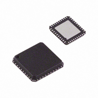
AD8339ACPZ Analog Devices Inc, AD8339ACPZ Datasheet - Page 24

AD8339ACPZ
Manufacturer Part Number
AD8339ACPZ
Description
IC I/Q DEMOD QUAD 50MHZ 40-LFCSP
Manufacturer
Analog Devices Inc
Datasheet
1.AD8339ACPZ.pdf
(36 pages)
Specifications of AD8339ACPZ
Function
Demodulator
Lo Frequency
0Hz ~ 200MHz
Rf Frequency
0Hz ~ 50MHz
P1db
14.8dBm
Gain
-1.3dB
Noise Figure
11.5dB
Current - Supply
35mA
Voltage - Supply
4.5 V ~ 5.5 V
Package / Case
40-VFQFN, 40-CSP, Exposed Pad
Frequency Range
DC To 50MHz
Rf Type
Quadrature
Supply Voltage Range
± 4.5V To ± 5.5V
Rf Ic Case Style
LFCSP
No. Of Pins
40
Operating Temperature Range
-40°C To +85°C
Lead Free Status / RoHS Status
Lead free / RoHS Compliant
For Use With
AD8339-EVALZ - BOARD EVAL AD8339 I/Q DEMOD
Lead Free Status / RoHS Status
Lead free / RoHS Compliant, Lead free / RoHS Compliant
Available stocks
Company
Part Number
Manufacturer
Quantity
Price
Company:
Part Number:
AD8339ACPZ
Manufacturer:
Analog Devices Inc
Quantity:
135
AD8339
APPLICATIONS INFORMATION
The AD8339 is the key component of a phase shifter system
that aligns time-skewed information contained in RF signals.
Combined with a variable gain amplifier (VGA) and a low noise
amplifier (LNA) as in the
family, the AD8339 forms a complete analog receiver for a high
performance ultrasound CW Doppler system.
LOGIC INPUTS AND INTERFACES
The SDI, SCLK, SDO, CSB, and RSET pins are CMOS com-
patible to 1.8 V. The threshold of the RSTS pin is 1.5 V with a
hysteresis of ±0.3 V. Each logic input pin is Schmitt trigger
activated, with a threshold centered at ~1.3 V and a hysteresis
of ±0.1 V around this value.
The only logic output, SDO, generates a signal that has a logic
low level of ~0.2 V and a logic high level of ~1.9 V to allow for
easy interfacing to the next AD8339 SDI input. Note that the
capacitive loading for the SDO pin should be kept as small as
possible (<5 pF), ideally only a short trace to the SDI pin of the
next chip. The output slew is limited to approximately ±500 μA,
which limits the speed when a large capacitor is connected.
Excessive values of parasitic capacitance on the SDO pin can
affect the timing and loading of data into the SDI input of the
next chip.
RESET INPUT
The RSET pin is used to synchronize the LO dividers in AD8339
arrays. Because they are driven by the same internal LO, the four
channels in any AD8339 are inherently synchronous. However,
when multiple AD8339s are used, it is possible that their dividers
wake up in different phase states. The function of the RSET pin
is to phase align all the LO signals in multiple AD8339s.
The 4LO divider of each AD8339 can be initiated in one of four
possible states: 0°, 90°, 180°, or 270° relative to other AD8339s.
The internally generated I/Q signals of each AD8339 LO are
always at a 90° angle relative to each other, but a phase shift can
occur during power-up between the dividers of multiple
AD8339s used in a common array.
The LO divider reset function has been improved in the AD8339
compared with the AD8333. The RSET pin still provides an
asynchronous reset of the LO dividers by forcing the internal
LO to hang; however, in the AD8339, the LO reset function is
fast and does not require a shutdown of the 4LO input signal.
AD8332/AD8334/AD8335
VGA
Rev. A | Page 24 of 36
The RSET mechanism also allows the measurement of non-
mixing gain from the RF input to the output. The rising edge of
the active high RSET pulse can occur at any time; however, the
duration should be ≥20 ns minimum. When the RSET pulse
transitions from high to low, the LO dividers are reactivated on
the next rising edge of the 4LO clock. To guarantee synchronous
operation of an array of AD8339s, the RSET pulse must go low
on all devices before the next rising edge of the 4LO clock.
Therefore, it is best to have the RSET pulse go low on the falling
edge of the 4LO clock; at the very least, the t
≥5 ns. An optimal timing setup is for the RSET pulse to go high
on a 4LO falling edge and to go low on a 4LO falling edge; this
gives 10 ns of setup time even at a 4LO frequency of 50 MHz
(12.5 MHz internal LO).
Check the synchronization of multiple AD8339s using the
following procedure:
1.
2.
3.
4.
5.
LO INPUT
The LO input is a high speed, fully differential analog input that
responds to differences in the input levels (and not logic levels).
The LO inputs can be driven with a low common-mode voltage
amplifier, such as the National Semiconductor® DS90C401 LVDS
driver. The graph in Figure 22 shows the range of common-mode
voltages. Logic families such as TTL or CMOS are unsuitable
for direct coupling to the LO input.
Activate at least one channel per AD8339 by setting the
appropriate channel enable bit in the serial interface.
Set the phase code of all AD8339 channels to the same
logic state, for example, 0000.
Apply the same test signal to all devices to generate a sine
wave in the baseband output and measure the output of
one channel per device.
Apply an RSET pulse to all AD8339s.
Because all the phase codes of the AD8339s should be the
same, the combined signal of multiple devices should be N
times greater than a single channel. If the combined signal
is less than N times one channel, one or more of the LO
phases of the individual AD8339s is in error.
SETUP
should be


