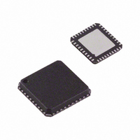
AD8339ACPZ Analog Devices Inc, AD8339ACPZ Datasheet - Page 23

AD8339ACPZ
Manufacturer Part Number
AD8339ACPZ
Description
IC I/Q DEMOD QUAD 50MHZ 40-LFCSP
Manufacturer
Analog Devices Inc
Datasheet
1.AD8339ACPZ.pdf
(36 pages)
Specifications of AD8339ACPZ
Function
Demodulator
Lo Frequency
0Hz ~ 200MHz
Rf Frequency
0Hz ~ 50MHz
P1db
14.8dBm
Gain
-1.3dB
Noise Figure
11.5dB
Current - Supply
35mA
Voltage - Supply
4.5 V ~ 5.5 V
Package / Case
40-VFQFN, 40-CSP, Exposed Pad
Frequency Range
DC To 50MHz
Rf Type
Quadrature
Supply Voltage Range
± 4.5V To ± 5.5V
Rf Ic Case Style
LFCSP
No. Of Pins
40
Operating Temperature Range
-40°C To +85°C
Lead Free Status / RoHS Status
Lead free / RoHS Compliant
For Use With
AD8339-EVALZ - BOARD EVAL AD8339 I/Q DEMOD
Lead Free Status / RoHS Status
Lead free / RoHS Compliant, Lead free / RoHS Compliant
Available stocks
Company
Part Number
Manufacturer
Quantity
Price
Company:
Part Number:
AD8339ACPZ
Manufacturer:
Analog Devices Inc
Quantity:
135
SERIAL INTERFACE
The AD8339 contains a 4-wire, SPI-compatible digital interface
(SDI, SCLK, CSB, and SDO). The interface comprises a 20-bit
shift register plus a latch. The shift register is loaded MSB first.
Phase selection and channel enabling information are contained
in the 20-bit word. Figure 56 is a bit map of the data-word, and
Figure 57 is the timing diagram.
The shift direction is to the right with MSB first. Because the
latch is implemented with D-flip-flops (DFF) and CSB acts as
the clock to the latch, any time that CSB is low, the latch flip-
flops monitor the shift register outputs. As soon as CSB goes
high, the data present in the register is latched. New data can be
loaded into the shift register at any time.
Twenty bits are required to program each AD8339; the data is
transferred from the register to the latch when CSB goes high.
Depending on the data, the corresponding channels are enabled,
and the phases are selected. Figure 57 illustrates the timing for
two sequentially programmed devices.
Note that the data is latched into the register flip-flops on the
rising edge of SCLK. SDO also transitions on the rising edge
of SCLK.
SCLK
SDO
CSB
REGISTER
SDI
LATCH
SHIFT
SCLK
RSTS
SDI
CSB
t
1
t
3
t
2
TO OTHER
AD8339s
TO OTHER
AD8339s
TO PHASE SELECT AND
CH 1
CH 1
LSB
LSB
CHANNEL ENABLES
BIAS BLOCKS FOR
ENABLE BITS
t
CH 2
CH 2
5
DATA FOR AD8339 #1
CH 3 CH 4
CH 3 CH 4
t
6
MSB
MSB
Figure 56. Serial Interface Showing the 20-Bit Shift Register and Latch
CH 1 CH 1 CH 1 CH 1 CH 2 CH 2 CH 2 CH 2
CH 1 CH 1 CH 1 CH 1 CH 2 CH 2 CH 2 CH 2
LSB
LSB
TO CHANNEL 1 PHASE
SELECT BLOCK
PH SEL CH 1
MSB
MSB
Figure 57. Timing Diagram
Rev. A | Page 23 of 36
LSB
LSB
TO CHANNEL 2 PHASE
t
SELECT BLOCK
4
PH SEL CH 2
ENBL BITS
When all four ENBL bits are low, only the SPI port is powered
up. This feature allows for low power consumption (~13 mW
per AD8339 or 3.25 mW per channel) when the CW Doppler
function is not needed. Because the SPI port stays alive even
with the rest of the chip powered down, the part can be awakened
again by simply programming the port. As soon as the CSB signal
goes high, the part turns on again. Note that this takes a fair
amount of time because of the external capacitor on the LODC
pin. It takes ~10 μs to 15 μs with the recommended 0.1 μF
decoupling capacitor. The decoupling capacitor on this pin is
intended to reduce bias noise contribution in the LO divider
chain. The user can experiment with the value of this decoupling
capacitor to determine the smallest value without degrading the
dynamic range within the frequency band of interest.
The SPI also has an additional pin that can be used in a test
mode or as a quick way to reset the SPI and depower the chip.
All bits in both the shift register and the latch are reset low
when the RSTS pin is pulled above ~1.5 V. For quick testing
without the need to program the SPI, the voltage on the RSTS
pin should be first pulled high and then pulled to −1.4 V. This
enables all four channels in the phase (I = 1, Q = 0) state (all
phase bits are 0000); the channel enable bits are all set to 1. This
is an untested threshold not intended for continuous operation.
MSB
MSB
CH 3 CH 3
CH 3 CH 3
LSB
LSB
TO CHANNEL 3 PHASE
SELECT BLOCK
PH SEL CH 3
DATA FOR AD8339 #2
CH 3 CH 3
CH 3 CH 3
MSB
MSB
CH 4
CH 4
LSB
LSB
TO CHANNEL 4 PHASE
SELECT BLOCK
PH SEL CH 4
CH 4
CH 4
CH 4 CH 4
CH 4 CH 4
MSB
MSB
SDO
TO NEXT
AD8339
t
7
AD8339
t
8


