HD6417032F20 Renesas Electronics America, HD6417032F20 Datasheet - Page 446
HD6417032F20
Manufacturer Part Number
HD6417032F20
Description
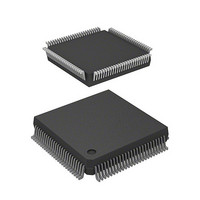
IC SUPERH MPU ROMLESS 112QFP
Manufacturer
Renesas Electronics America
Series
SuperH® SH7030r
Datasheet
1.HD6417034AFI20.pdf
(689 pages)
Specifications of HD6417032F20
Core Processor
SH-1
Core Size
32-Bit
Speed
20MHz
Connectivity
EBI/EMI, SCI
Peripherals
DMA, POR, PWM, WDT
Number Of I /o
32
Program Memory Type
ROMless
Ram Size
4K x 8
Voltage - Supply (vcc/vdd)
4.5 V ~ 5.5 V
Data Converters
A/D 8x10b
Oscillator Type
Internal
Operating Temperature
-20°C ~ 75°C
Package / Case
112-QFP
Lead Free Status / RoHS Status
Contains lead / RoHS non-compliant
Eeprom Size
-
Program Memory Size
-
Available stocks
Company
Part Number
Manufacturer
Quantity
Price
Company:

Part Number:
HD6417032F20
Manufacturer:
HIT
Quantity:
5 510
Company:
Part Number:
HD6417032F20
Manufacturer:
AMCC
Quantity:
5 510
Company:
Part Number:
HD6417032F20
Manufacturer:
Renesas Electronics America
Quantity:
10 000
Part Number:
HD6417032F20
Manufacturer:
HITACHI/日立
Quantity:
20 000
Company:
Part Number:
HD6417032F20V
Manufacturer:
TI
Quantity:
201


Section 14 A/D Converter
Bit 7—Trigger Enable (TRGE): TRGE selects whether or not to start A/D conversion when an
external trigger is input.
Bit 7 (TRGE)
0
1
Bits 6–0—Reserved): These bits are always read as 1. The write value should always be 1.
14.3
The A/D data registers (ADDRA–ADDRD) are 16-bit registers, but they are connected to the CPU
by an 8-bit data bus. Therefore, the upper byte of each register can be read directly, but the lower
byte is accessed through an 8-bit temporary register (TEMP).
When the CPU reads the upper byte of an A/D data register, the upper byte is transferred to the
CPU and the lower byte to TEMP. When the lower byte is accessed, the value in TEMP is
transferred to the CPU.
A program should first read the upper byte, then the lower byte of the A/D data register. This can
be performed by reading ADDR from the upper byte end using a word transfer instruction
(MOV.W, etc.). Reading only the upper byte would assure the CPU of obtaining consistent data. If
the program reads only the lower byte, however, consistent data will not be guaranteed.
Figure 14.2 shows the data flow during access to A/D data registers.
Rev. 7.00 Jan 31, 2006 page 418 of 658
REJ09B0272-0700
CPU Interface
Description
When an external trigger is input, A/D conversion does not start
A/D conversion starts at the falling edge of an input signal from the external
trigger pin (ADTRG).
(Initial value)
Related parts for HD6417032F20
Image
Part Number
Description
Manufacturer
Datasheet
Request
R

Part Number:
Description:
KIT STARTER FOR M16C/29
Manufacturer:
Renesas Electronics America
Datasheet:

Part Number:
Description:
KIT STARTER FOR R8C/2D
Manufacturer:
Renesas Electronics America
Datasheet:

Part Number:
Description:
R0K33062P STARTER KIT
Manufacturer:
Renesas Electronics America
Datasheet:

Part Number:
Description:
KIT STARTER FOR R8C/23 E8A
Manufacturer:
Renesas Electronics America
Datasheet:

Part Number:
Description:
KIT STARTER FOR R8C/25
Manufacturer:
Renesas Electronics America
Datasheet:

Part Number:
Description:
KIT STARTER H8S2456 SHARPE DSPLY
Manufacturer:
Renesas Electronics America
Datasheet:

Part Number:
Description:
KIT STARTER FOR R8C38C
Manufacturer:
Renesas Electronics America
Datasheet:

Part Number:
Description:
KIT STARTER FOR R8C35C
Manufacturer:
Renesas Electronics America
Datasheet:

Part Number:
Description:
KIT STARTER FOR R8CL3AC+LCD APPS
Manufacturer:
Renesas Electronics America
Datasheet:
Part Number:
Description:
KIT STARTER FOR RX610
Manufacturer:
Renesas Electronics America
Datasheet:

Part Number:
Description:
KIT STARTER FOR R32C/118
Manufacturer:
Renesas Electronics America
Datasheet:

Part Number:
Description:
KIT DEV RSK-R8C/26-29
Manufacturer:
Renesas Electronics America
Datasheet:

Part Number:
Description:
KIT STARTER FOR SH7124
Manufacturer:
Renesas Electronics America
Datasheet:

Part Number:
Description:
KIT STARTER FOR H8SX/1622
Manufacturer:
Renesas Electronics America
Datasheet:

Part Number:
Description:
KIT DEV FOR SH7203
Manufacturer:
Renesas Electronics America
Datasheet: