HD6417032F20 Renesas Electronics America, HD6417032F20 Datasheet - Page 250
HD6417032F20
Manufacturer Part Number
HD6417032F20
Description
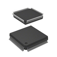
IC SUPERH MPU ROMLESS 112QFP
Manufacturer
Renesas Electronics America
Series
SuperH® SH7030r
Datasheet
1.HD6417034AFI20.pdf
(689 pages)
Specifications of HD6417032F20
Core Processor
SH-1
Core Size
32-Bit
Speed
20MHz
Connectivity
EBI/EMI, SCI
Peripherals
DMA, POR, PWM, WDT
Number Of I /o
32
Program Memory Type
ROMless
Ram Size
4K x 8
Voltage - Supply (vcc/vdd)
4.5 V ~ 5.5 V
Data Converters
A/D 8x10b
Oscillator Type
Internal
Operating Temperature
-20°C ~ 75°C
Package / Case
112-QFP
Lead Free Status / RoHS Status
Contains lead / RoHS non-compliant
Eeprom Size
-
Program Memory Size
-
Available stocks
Company
Part Number
Manufacturer
Quantity
Price
Company:

Part Number:
HD6417032F20
Manufacturer:
HIT
Quantity:
5 510
Company:
Part Number:
HD6417032F20
Manufacturer:
AMCC
Quantity:
5 510
Company:
Part Number:
HD6417032F20
Manufacturer:
Renesas Electronics America
Quantity:
10 000
Part Number:
HD6417032F20
Manufacturer:
HITACHI/日立
Quantity:
20 000
Company:
Part Number:
HD6417032F20V
Manufacturer:
TI
Quantity:
201


Section 9 Direct Memory Access Controller (DMAC)
8. When the following operations are performed in the order shown when the pin to which DREQ
Rev. 7.00 Jan 31, 2006 page 222 of 658
REJ09B0272-0700
Especially, if, as shown in figure 9.26, the DMA bus cycle is a full access to DRAM or if a
refresh request is generated, sampling of DREQ takes place before DACK is output as
mentioned above. This phenomenon is found when one of the following transfers is made with
DREQ set to level detection in DMA cycle-steal mode, in a system which employs DRAM
(refresh enabled).
Remedy:
To prevent unnecessary DMA transfers, configure the system so that DREQ is edge-detected
and the edge corresponding to the next transfer request occurs after DACK output.
input is assigned is designated as a general input pin by the pin function controller (PFC) and
inputs a low-level signal, the DREQ falling edge is detected, and a DMA transfer request
accepted, immediately after the setting in (b) is performed:
a. A channel control register (CHCRn) setting is made so that an interrupt is detected at the
b.
Therefore, when switching the pin function from general input pin to DREQ input, the pin
function controller (PFC) setting should be changed to DREQ input while the pin to which
DREQ input is assigned is high.
DACK
Transfer from a device with DACK to memory in single address mode (not restricted to
DRAM)
Transfer from DRAM to a device with DACK in single address mode
Output at DACK write in dual address mode
Output at DACK read in dual address mode and DMA transfer using DRAM as the source
falling edge of DREQ.
The function of the pin to which DREQ input is assigned is switched from general input to
DREQ input by a pin function controller (PFC) setting.
CK
DRAM bus cycle
Figure 9.26 Example of DREQ
Tp
Sampling point
(Full access)
Tr
Tc
Refresh
Sampling point
When refresh operation is entered
Sampling point of DREQ for DACK output position
differs with presence/absence of the refresh operation.
DREQ Sampling before Output of DACK
DREQ
DREQ
T1
T2
Related parts for HD6417032F20
Image
Part Number
Description
Manufacturer
Datasheet
Request
R

Part Number:
Description:
KIT STARTER FOR M16C/29
Manufacturer:
Renesas Electronics America
Datasheet:

Part Number:
Description:
KIT STARTER FOR R8C/2D
Manufacturer:
Renesas Electronics America
Datasheet:

Part Number:
Description:
R0K33062P STARTER KIT
Manufacturer:
Renesas Electronics America
Datasheet:

Part Number:
Description:
KIT STARTER FOR R8C/23 E8A
Manufacturer:
Renesas Electronics America
Datasheet:

Part Number:
Description:
KIT STARTER FOR R8C/25
Manufacturer:
Renesas Electronics America
Datasheet:

Part Number:
Description:
KIT STARTER H8S2456 SHARPE DSPLY
Manufacturer:
Renesas Electronics America
Datasheet:

Part Number:
Description:
KIT STARTER FOR R8C38C
Manufacturer:
Renesas Electronics America
Datasheet:

Part Number:
Description:
KIT STARTER FOR R8C35C
Manufacturer:
Renesas Electronics America
Datasheet:

Part Number:
Description:
KIT STARTER FOR R8CL3AC+LCD APPS
Manufacturer:
Renesas Electronics America
Datasheet:
Part Number:
Description:
KIT STARTER FOR RX610
Manufacturer:
Renesas Electronics America
Datasheet:

Part Number:
Description:
KIT STARTER FOR R32C/118
Manufacturer:
Renesas Electronics America
Datasheet:

Part Number:
Description:
KIT DEV RSK-R8C/26-29
Manufacturer:
Renesas Electronics America
Datasheet:

Part Number:
Description:
KIT STARTER FOR SH7124
Manufacturer:
Renesas Electronics America
Datasheet:

Part Number:
Description:
KIT STARTER FOR H8SX/1622
Manufacturer:
Renesas Electronics America
Datasheet:

Part Number:
Description:
KIT DEV FOR SH7203
Manufacturer:
Renesas Electronics America
Datasheet: