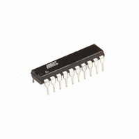
ATTINY26-16PI Atmel, ATTINY26-16PI Datasheet - Page 7

ATTINY26-16PI
Manufacturer Part Number
ATTINY26-16PI
Description
IC AVR MCU 2K 16MHZ IND 20-DIP
Manufacturer
Atmel
Series
AVR® ATtinyr
Specifications of ATTINY26-16PI
Core Processor
AVR
Core Size
8-Bit
Speed
16MHz
Connectivity
USI
Peripherals
Brown-out Detect/Reset, POR, PWM, WDT
Number Of I /o
16
Program Memory Size
2KB (1K x 16)
Program Memory Type
FLASH
Eeprom Size
128 x 8
Ram Size
128 x 8
Voltage - Supply (vcc/vdd)
4.5 V ~ 5.5 V
Data Converters
A/D 11x10b
Oscillator Type
Internal
Operating Temperature
-40°C ~ 85°C
Package / Case
20-DIP (0.300", 7.62mm)
Lead Free Status / RoHS Status
Contains lead / RoHS non-compliant
- Current page: 7 of 182
- Download datasheet (3Mb)
AVR CPU Core
Architectural
Overview
1477K–AVR–08/10
The fast-access Register File concept contains 32 x 8-bit general purpose working registers with
a single clock cycle access time. This means that during one single clock cycle, one ALU (Arith-
metic Logic Unit) operation is executed. Two operands are output from the Register File, the
operation is executed, and the result is stored back in the Register File – in one clock cycle.
Six of the 32 registers can be used as 16-bit pointers for indirect memory access. These pointers
are called the X-, Y-, and Z-pointers, and they can address the Register File and the Flash pro-
gram memory.
Figure 2. The ATtiny26(L) AVR Enhanced RISC Architecture
The ALU supports arithmetic and logic functions between registers or between a constant and a
register. Single register operations are also executed in the ALU. Figure 2 shows the
ATtiny26(L) AVR Enhanced RISC microcontroller architecture. In addition to the register opera-
tion, the conventional memory addressing modes can be used on the Register File as well. This
is enabled by the fact that the Register File is assigned the 32 lowermost Data Space addresses
($00 - $1F), allowing them to be accessed as though they were ordinary memory locations.
The I/O memory space contains 64 addresses for CPU peripheral functions as Control Regis-
ters, Timer/Counters, A/D Converters, and other I/O functions. The I/O Memory can be
accessed directly, or as the Data Space locations following those of the Register File, $20 - $5F.
The AVR uses a Harvard architecture concept with separate memories and buses for program
and data memories. The program memory is accessed with a two stage pipelining. While one
instruction is being executed, the next instruction is pre-fetched from the program memory. This
Control Lines
Instruction
1024 x 16
Instruction
Program
Register
Decoder
FLASH
Program
Counter
EEPROM
Registers
128 byte
128 x 8
and Test
Purpose
General
SRAM
8-bit Data Bus
Status
32 x 8
ALU
Serial Interface
Timer/Counter
Comparator
Registers
Watchdog
Universal
2 x 8-bit
Interrupt
ISP Unit
I/O Lines
Control
Analog
ADC
Timer
Unit
7
Related parts for ATTINY26-16PI
Image
Part Number
Description
Manufacturer
Datasheet
Request
R

Part Number:
Description:
Manufacturer:
Atmel Corporation
Datasheet:

Part Number:
Description:
IC AVR MCU 2K 16MHZ IND 32-QFN
Manufacturer:
Atmel
Datasheet:

Part Number:
Description:
IC AVR MCU 2K 16MHZ IND 20-SOIC
Manufacturer:
Atmel
Datasheet:

Part Number:
Description:
IC AVR MCU 2K 16MHZ IND 20-DIP
Manufacturer:
Atmel
Datasheet:

Part Number:
Description:
IC AVR MCU 2K 16MHZ IND 32-QFN
Manufacturer:
Atmel
Datasheet:

Part Number:
Description:
IC AVR MCU 2K 16MHZ COM 20-SOIC
Manufacturer:
Atmel
Datasheet:

Part Number:
Description:
IC AVR MCU 2K 16MHZ IND 20-SOIC
Manufacturer:
Atmel
Datasheet:

Part Number:
Description:
ID MCU AVR 2K 5V 16MHZ 32-QFN
Manufacturer:
Atmel
Datasheet:

Part Number:
Description:
Microcontrollers (MCU) AVR 2K FLASH 128B EE 128B SRAM ADC
Manufacturer:
Atmel
Datasheet:

Part Number:
Description:
IC AVR MCU 2K 16MHZ COM 32-QFN
Manufacturer:
Atmel
Datasheet:

Part Number:
Description:
IC AVR MCU 2K 16MHZ COM 20-DIP
Manufacturer:
Atmel
Datasheet:

Part Number:
Description:
ID MCU AVR 2K 5V 16MHZ 20-DIP
Manufacturer:
Atmel
Datasheet:

Part Number:
Description:
ID MCU AVR 2K 5V 16MHZ 20-SOIC
Manufacturer:
Atmel
Datasheet:

Part Number:
Description:
IC MCU AVR 2K 16MHZ IND 20SOIC
Manufacturer:
Atmel
Datasheet:


