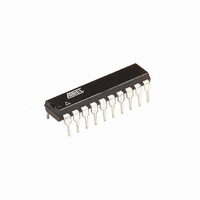
ATTINY26-16PI Atmel, ATTINY26-16PI Datasheet - Page 67

ATTINY26-16PI
Manufacturer Part Number
ATTINY26-16PI
Description
IC AVR MCU 2K 16MHZ IND 20-DIP
Manufacturer
Atmel
Series
AVR® ATtinyr
Specifications of ATTINY26-16PI
Core Processor
AVR
Core Size
8-Bit
Speed
16MHz
Connectivity
USI
Peripherals
Brown-out Detect/Reset, POR, PWM, WDT
Number Of I /o
16
Program Memory Size
2KB (1K x 16)
Program Memory Type
FLASH
Eeprom Size
128 x 8
Ram Size
128 x 8
Voltage - Supply (vcc/vdd)
4.5 V ~ 5.5 V
Data Converters
A/D 11x10b
Oscillator Type
Internal
Operating Temperature
-40°C ~ 85°C
Package / Case
20-DIP (0.300", 7.62mm)
Lead Free Status / RoHS Status
Contains lead / RoHS non-compliant
- Current page: 67 of 182
- Download datasheet (3Mb)
Timer/Counter0 –
TCNT0
8-bit
Timer/Counter1
1477K–AVR–08/10
The Stop condition provides a Timer Enable/Disable function. The CK down divided modes are
scaled directly from the CK oscillator clock. If the external pin modes are used, the correspond-
ing setup must be performed in the actual Data Direction Control Register (cleared to zero gives
an input pin).
The Timer/Counter0 is implemented as an up-counter with read and write access. If the
Timer/Counter0 is written and a clock source is present, the Timer/Counter0 continues counting
in the timer clock cycle following the write operation.
The Timer/Counter1 has two clocking modes: a synchronous mode and an asynchronous mode.
The synchronous mode uses the system clock (CK) as the clock timebase and asynchronous
mode uses the fast peripheral clock (PCK) as the clock time base. The PCKE bit from the
PLLCSR Register enables the asynchronous mode when it is set (“1”). The Timer/Counter1 gen-
eral operation is described in the asynchronous mode and the operation in the synchronous
mode is mentioned only if there is differences between these two modes. Figure 39 shows
Timer/Counter1 synchronization register block diagram and synchronization delays in between
registers. Note that all clock gating details are not shown in the figure. The Timer/Counter1 Reg-
ister values go through the internal synchronization registers, which cause the input
synchronization delay, before affecting the counter operation. The registers TCCR1A, TCCR1B,
OCR1A, OCR1B, and OCR1C can be read back right after writing the register. The read back
values are delayed for the Timer/Counter1 (TCNT1) Register and flags (OCF1A, OCF1B, and
TOV1), because of the input and output synchronization.
This module features a high resolution and a high accuracy usage with the lower prescaling
opportunities. Timer/Counter1 can also support two accurate, high speed, 8-bit Pulse Width
Modulators using clock speeds up to 64 MHz. In this mode, Timer/Counter1 and the Output
Compare Registers serve as dual stand-alone PWMs with non-overlapping non-inverted and
inverted outputs. Refer to page 74 for a detailed description on this function. Similarly, the high
prescaling opportunities make this unit useful for lower speed functions or exact timing functions
with infrequent actions.
Bit
$32 ($52)
Read/Write
Initial Value
MSB
R/W
7
0
R/W
6
0
R/W
5
0
R/W
4
0
R/W
3
0
R/W
2
0
R/W
1
0
LSB
R/W
0
0
TCNT0
67
Related parts for ATTINY26-16PI
Image
Part Number
Description
Manufacturer
Datasheet
Request
R

Part Number:
Description:
Manufacturer:
Atmel Corporation
Datasheet:

Part Number:
Description:
IC AVR MCU 2K 16MHZ IND 32-QFN
Manufacturer:
Atmel
Datasheet:

Part Number:
Description:
IC AVR MCU 2K 16MHZ IND 20-SOIC
Manufacturer:
Atmel
Datasheet:

Part Number:
Description:
IC AVR MCU 2K 16MHZ IND 20-DIP
Manufacturer:
Atmel
Datasheet:

Part Number:
Description:
IC AVR MCU 2K 16MHZ IND 32-QFN
Manufacturer:
Atmel
Datasheet:

Part Number:
Description:
IC AVR MCU 2K 16MHZ COM 20-SOIC
Manufacturer:
Atmel
Datasheet:

Part Number:
Description:
IC AVR MCU 2K 16MHZ IND 20-SOIC
Manufacturer:
Atmel
Datasheet:

Part Number:
Description:
ID MCU AVR 2K 5V 16MHZ 32-QFN
Manufacturer:
Atmel
Datasheet:

Part Number:
Description:
Microcontrollers (MCU) AVR 2K FLASH 128B EE 128B SRAM ADC
Manufacturer:
Atmel
Datasheet:

Part Number:
Description:
IC AVR MCU 2K 16MHZ COM 32-QFN
Manufacturer:
Atmel
Datasheet:

Part Number:
Description:
IC AVR MCU 2K 16MHZ COM 20-DIP
Manufacturer:
Atmel
Datasheet:

Part Number:
Description:
ID MCU AVR 2K 5V 16MHZ 20-DIP
Manufacturer:
Atmel
Datasheet:

Part Number:
Description:
ID MCU AVR 2K 5V 16MHZ 20-SOIC
Manufacturer:
Atmel
Datasheet:

Part Number:
Description:
IC MCU AVR 2K 16MHZ IND 20SOIC
Manufacturer:
Atmel
Datasheet:


