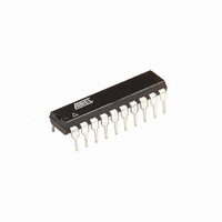
ATTINY26-16PI Atmel, ATTINY26-16PI Datasheet - Page 40

ATTINY26-16PI
Manufacturer Part Number
ATTINY26-16PI
Description
IC AVR MCU 2K 16MHZ IND 20-DIP
Manufacturer
Atmel
Series
AVR® ATtinyr
Specifications of ATTINY26-16PI
Core Processor
AVR
Core Size
8-Bit
Speed
16MHz
Connectivity
USI
Peripherals
Brown-out Detect/Reset, POR, PWM, WDT
Number Of I /o
16
Program Memory Size
2KB (1K x 16)
Program Memory Type
FLASH
Eeprom Size
128 x 8
Ram Size
128 x 8
Voltage - Supply (vcc/vdd)
4.5 V ~ 5.5 V
Data Converters
A/D 11x10b
Oscillator Type
Internal
Operating Temperature
-40°C ~ 85°C
Package / Case
20-DIP (0.300", 7.62mm)
Lead Free Status / RoHS Status
Contains lead / RoHS non-compliant
- Current page: 40 of 182
- Download datasheet (3Mb)
Minimizing Power
Consumption
Analog to Digital
Converter
Analog Comparator
Brown-out Detector
Internal Voltage
Reference
Watchdog Timer
Port Pins
40
ATtiny26(L)
There are several issues to consider when trying to minimize the power consumption in an AVR
controlled system. In general, sleep modes should be used as much as possible, and the sleep
mode should be selected so that as few as possible of the device’s functions are operating. All
functions not needed should be disabled. In particular, the following modules may need special
consideration when trying to achieve the lowest possible power consumption.
If enabled, the ADC will be enabled in all sleep modes. To save power, the ADC should be dis-
abled before entering any sleep mode. When the ADC is turned off and on again, the next
conversion will be an extended conversion. Refer to “Analog to Digital Converter” on page 94 for
details on ADC operation.
When entering Idle mode, the Analog Comparator should be disabled if not used. When entering
ADC Noise Reduction mode, the Analog Comparator should be disabled. In the other sleep
modes, the Analog Comparator is automatically disabled. However, if the Analog Comparator is
set up to use the Internal Voltage Reference as input, the Analog Comparator should be dis-
abled in all sleep modes. Otherwise, the Internal Voltage Reference will be enabled,
independent of sleep mode. Refer to “Analog Comparator” on page 91 for details on how to con-
figure the Analog Comparator.
If the Brown-out Detector is not needed in the application, this module should be turned off. If the
Brown-out Detector is enabled by the BODEN Fuse, it will be enabled in all sleep modes, and
hence, always consume power. In the deeper sleep modes, this will contribute significantly to
the total current consumption. Refer to “Brown-out Detection” on page 35 for details on how to
configure the Brown-out Detector.
The Internal Voltage Reference (see Table 20) will be enabled when needed by the Brown-out
Detector, the Analog Comparator or the ADC. If these modules are disabled as described in the
sections above, the Internal Voltage Reference will be disabled and it will not be consuming
power. When turned on again, the user must allow the reference to start up before the output is
used. If the reference is kept on in sleep mode, the output can be used immediately.
Table 20. Internal Voltage Reference
If the Watchdog Timer is not needed in the application, this module should be turned off. If the
Watchdog Timer is enabled, it will be enabled in all sleep modes, and hence, always consume
power. In the deeper sleep modes, this will contribute significantly to the total current consump-
tion. Refer to “Watchdog Timer” on page 78 for details on how to configure the Watchdog Timer.
When entering a sleep mode, all port pins should be configured to use minimum power. The
most important thing is then to ensure that no pins drive resistive loads. In sleep modes where
the both the I/O clock (clk
device will be disabled. This ensures that no power is consumed by the input logic when not
needed. In some cases, the input logic is needed for detecting wake-up conditions, and it will
then be enabled. Refer to “Digital Input Enable and Sleep Modes” on page 45 for details on
which pins are enabled. If the input buffer is enabled and the input signal is left floating or have
an analog signal level close to V
Symbol
V
t
I
BG
BG
BG
Parameter
Bandgap reference voltage
Bandgap reference start-up time
Bandgap reference current consumption
I/O
) and the ADC clock (clk
CC
/2, the input buffer will use excessive power.
ADC
1.15
Min
) are stopped, the input buffers of the
1.18
Typ
40
10
Max
1.40
70
Units
µA
1477K–AVR–08/10
µs
V
Related parts for ATTINY26-16PI
Image
Part Number
Description
Manufacturer
Datasheet
Request
R

Part Number:
Description:
Manufacturer:
Atmel Corporation
Datasheet:

Part Number:
Description:
IC AVR MCU 2K 16MHZ IND 32-QFN
Manufacturer:
Atmel
Datasheet:

Part Number:
Description:
IC AVR MCU 2K 16MHZ IND 20-SOIC
Manufacturer:
Atmel
Datasheet:

Part Number:
Description:
IC AVR MCU 2K 16MHZ IND 20-DIP
Manufacturer:
Atmel
Datasheet:

Part Number:
Description:
IC AVR MCU 2K 16MHZ IND 32-QFN
Manufacturer:
Atmel
Datasheet:

Part Number:
Description:
IC AVR MCU 2K 16MHZ COM 20-SOIC
Manufacturer:
Atmel
Datasheet:

Part Number:
Description:
IC AVR MCU 2K 16MHZ IND 20-SOIC
Manufacturer:
Atmel
Datasheet:

Part Number:
Description:
ID MCU AVR 2K 5V 16MHZ 32-QFN
Manufacturer:
Atmel
Datasheet:

Part Number:
Description:
Microcontrollers (MCU) AVR 2K FLASH 128B EE 128B SRAM ADC
Manufacturer:
Atmel
Datasheet:

Part Number:
Description:
IC AVR MCU 2K 16MHZ COM 32-QFN
Manufacturer:
Atmel
Datasheet:

Part Number:
Description:
IC AVR MCU 2K 16MHZ COM 20-DIP
Manufacturer:
Atmel
Datasheet:

Part Number:
Description:
ID MCU AVR 2K 5V 16MHZ 20-DIP
Manufacturer:
Atmel
Datasheet:

Part Number:
Description:
ID MCU AVR 2K 5V 16MHZ 20-SOIC
Manufacturer:
Atmel
Datasheet:

Part Number:
Description:
IC MCU AVR 2K 16MHZ IND 20SOIC
Manufacturer:
Atmel
Datasheet:


