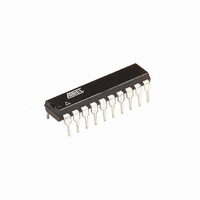
ATTINY26-16PI Atmel, ATTINY26-16PI Datasheet - Page 53

ATTINY26-16PI
Manufacturer Part Number
ATTINY26-16PI
Description
IC AVR MCU 2K 16MHZ IND 20-DIP
Manufacturer
Atmel
Series
AVR® ATtinyr
Specifications of ATTINY26-16PI
Core Processor
AVR
Core Size
8-Bit
Speed
16MHz
Connectivity
USI
Peripherals
Brown-out Detect/Reset, POR, PWM, WDT
Number Of I /o
16
Program Memory Size
2KB (1K x 16)
Program Memory Type
FLASH
Eeprom Size
128 x 8
Ram Size
128 x 8
Voltage - Supply (vcc/vdd)
4.5 V ~ 5.5 V
Data Converters
A/D 11x10b
Oscillator Type
Internal
Operating Temperature
-40°C ~ 85°C
Package / Case
20-DIP (0.300", 7.62mm)
Lead Free Status / RoHS Status
Contains lead / RoHS non-compliant
- Current page: 53 of 182
- Download datasheet (3Mb)
ATtiny26(L)
PCINT0: Pin Change Interrupt 0 pin. Pin change interrupt is enabled on pin when global interrupt
is enabled, pin change interrupt is enabled and the alternate functions do not mask the interrupt.
The masking alternate function is the output compare match output OC1B. Digital input is
enabled on pin PB3 also in SLEEP modes, if the pin change interrupt is enabled and not masked
by the alternate functions.
• SCK/SCL/OC1B/PCINT0 – Port B, Bit 2
SCK: Clock input or output in USI Three-wire mode. When the SPI is enabled this pin is config-
ured as an input. In the USI Three-wire mode the bit DDRB2 controls the direction of the pin,
output for the Master mode and input for the Slave mode.
SCL: USI External Open-collector Serial Clock for USI Two-wire mode. The SCL pin is pulled
low when PORTB2 is cleared (zero) or USI start condition is detected and DDRB2 is set (one).
Pull-up is disabled in USI Two-wire mode.
OC1B: Inverted Timer/Counter1 PWM Output B: The PB2 pin can serve as an inverted output
for the Timer/Counter1 PWM mode if USI is not enabled. The PB2 pin has to be configured as
an output (DDB2 set (one)) to serve this function.
PCINT1: Pin Change Interrupt 0 pin. Pin change interrupt is enabled on pin when global interrupt
is enabled, pin change interrupt is enabled and the alternate functions do not mask the interrupt.
The masking alternate function are the inverted output compare match output OC1B and USI
clocks SCK/SCL. Digital input is enabled on pin PB2 also in SLEEP modes, if the pin change
interrupt is enabled and not masked by the alternate functions.
• DO/OC1A/PCINT0 – Port B, Bit 1
DO: Data Output in USI Three-wire mode. Data output (DO) overrides PORTB1 value and it is
driven to the port when the data direction bit DDB1 is set (one). However the PORTB1 bit still
controls the pullup, enabling pullup if direction is input and PORTB1 is set(one).
OC1A: Output Compare match output: The PB1 pin can serve as an output for the
Timer/Counter1 compare match A. The PB1 pin has to be configured as an output (DDB1 set
(one)) to serve this function. The OC1B pin is also the output pin for the PWM mode timer func-
tion if not used in programming or USI.
PCINT0: Pin Change Interrupt 0 pin. Pin change interrupt is enabled on pin when global interrupt
is enabled, pin change interrupt is enabled and the alternate functions do not mask the interrupt.
The masking alternate functions are the output compare match output OC1A and Data Output
(DO) in USI Three-wire mode. Digital input is enabled on pin PB1 also in SLEEP modes, if the
pin change interrupt is enabled and not masked by the alternate functions.
53
1477K–AVR–08/10
Related parts for ATTINY26-16PI
Image
Part Number
Description
Manufacturer
Datasheet
Request
R

Part Number:
Description:
Manufacturer:
Atmel Corporation
Datasheet:

Part Number:
Description:
IC AVR MCU 2K 16MHZ IND 32-QFN
Manufacturer:
Atmel
Datasheet:

Part Number:
Description:
IC AVR MCU 2K 16MHZ IND 20-SOIC
Manufacturer:
Atmel
Datasheet:

Part Number:
Description:
IC AVR MCU 2K 16MHZ IND 20-DIP
Manufacturer:
Atmel
Datasheet:

Part Number:
Description:
IC AVR MCU 2K 16MHZ IND 32-QFN
Manufacturer:
Atmel
Datasheet:

Part Number:
Description:
IC AVR MCU 2K 16MHZ COM 20-SOIC
Manufacturer:
Atmel
Datasheet:

Part Number:
Description:
IC AVR MCU 2K 16MHZ IND 20-SOIC
Manufacturer:
Atmel
Datasheet:

Part Number:
Description:
ID MCU AVR 2K 5V 16MHZ 32-QFN
Manufacturer:
Atmel
Datasheet:

Part Number:
Description:
Microcontrollers (MCU) AVR 2K FLASH 128B EE 128B SRAM ADC
Manufacturer:
Atmel
Datasheet:

Part Number:
Description:
IC AVR MCU 2K 16MHZ COM 32-QFN
Manufacturer:
Atmel
Datasheet:

Part Number:
Description:
IC AVR MCU 2K 16MHZ COM 20-DIP
Manufacturer:
Atmel
Datasheet:

Part Number:
Description:
ID MCU AVR 2K 5V 16MHZ 20-DIP
Manufacturer:
Atmel
Datasheet:

Part Number:
Description:
ID MCU AVR 2K 5V 16MHZ 20-SOIC
Manufacturer:
Atmel
Datasheet:

Part Number:
Description:
IC MCU AVR 2K 16MHZ IND 20SOIC
Manufacturer:
Atmel
Datasheet:


