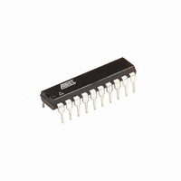
ATTINY26-16PI Atmel, ATTINY26-16PI Datasheet - Page 11

ATTINY26-16PI
Manufacturer Part Number
ATTINY26-16PI
Description
IC AVR MCU 2K 16MHZ IND 20-DIP
Manufacturer
Atmel
Series
AVR® ATtinyr
Specifications of ATTINY26-16PI
Core Processor
AVR
Core Size
8-Bit
Speed
16MHz
Connectivity
USI
Peripherals
Brown-out Detect/Reset, POR, PWM, WDT
Number Of I /o
16
Program Memory Size
2KB (1K x 16)
Program Memory Type
FLASH
Eeprom Size
128 x 8
Ram Size
128 x 8
Voltage - Supply (vcc/vdd)
4.5 V ~ 5.5 V
Data Converters
A/D 11x10b
Oscillator Type
Internal
Operating Temperature
-40°C ~ 85°C
Package / Case
20-DIP (0.300", 7.62mm)
Lead Free Status / RoHS Status
Contains lead / RoHS non-compliant
- Current page: 11 of 182
- Download datasheet (3Mb)
Stack Pointer – SP
Program and Data
Addressing Modes
Register Direct, Single
Register Rd
Register Direct, Two
Registers Rd and Rr
1477K–AVR–08/10
The ATtiny26(L) Stack Pointer is implemented as an 8-bit register in the I/O space location $3D
($5D). As the ATtiny26(L) data memory has 224 ($E0) locations, eight bits are used.
The Stack Pointer points to the data SRAM stack area where the Subroutine and Interrupt
Stacks are located. This Stack space in the data SRAM must be defined by the program before
any subroutine calls are executed or interrupts are enabled. The Stack Pointer must be set to
point above $60. The Stack Pointer is decremented by one when data is pushed onto the Stack
with the PUSH instruction, and it is decremented by two when an address is pushed onto the
Stack with subroutine calls and interrupts. The Stack Pointer is incremented by one when data is
popped from the Stack with the POP instruction, and it is incremented by two when an address
is popped from the Stack with return from subroutine RET or return from interrupt RETI.
The ATtiny26(L) AVR Enhanced RISC microcontroller supports powerful and efficient address-
ing modes for access to the Flash program memory, SRAM, Register File, and I/O Data
memory. This section describes the different addressing modes supported by the AVR architec-
ture. In the figures, OP means the operation code part of the instruction word. To simplify, not all
figures show the exact location of the addressing bits.
Figure 5. Direct Single Register Addressing
The operand is contained in register d (Rd).
Figure 6. Direct Register Addressing, Two Registers
Bit
$3D ($5D)
Read/Write
Initial Value
R/W
SP7
7
0
SP6
R/W
6
0
SP5
R/W
5
0
R/W
SP4
4
0
R/W
SP3
3
0
SP2
R/W
2
0
SP1
R/W
1
0
SP0
R/W
0
0
SP
11
Related parts for ATTINY26-16PI
Image
Part Number
Description
Manufacturer
Datasheet
Request
R

Part Number:
Description:
Manufacturer:
Atmel Corporation
Datasheet:

Part Number:
Description:
IC AVR MCU 2K 16MHZ IND 32-QFN
Manufacturer:
Atmel
Datasheet:

Part Number:
Description:
IC AVR MCU 2K 16MHZ IND 20-SOIC
Manufacturer:
Atmel
Datasheet:

Part Number:
Description:
IC AVR MCU 2K 16MHZ IND 20-DIP
Manufacturer:
Atmel
Datasheet:

Part Number:
Description:
IC AVR MCU 2K 16MHZ IND 32-QFN
Manufacturer:
Atmel
Datasheet:

Part Number:
Description:
IC AVR MCU 2K 16MHZ COM 20-SOIC
Manufacturer:
Atmel
Datasheet:

Part Number:
Description:
IC AVR MCU 2K 16MHZ IND 20-SOIC
Manufacturer:
Atmel
Datasheet:

Part Number:
Description:
ID MCU AVR 2K 5V 16MHZ 32-QFN
Manufacturer:
Atmel
Datasheet:

Part Number:
Description:
Microcontrollers (MCU) AVR 2K FLASH 128B EE 128B SRAM ADC
Manufacturer:
Atmel
Datasheet:

Part Number:
Description:
IC AVR MCU 2K 16MHZ COM 32-QFN
Manufacturer:
Atmel
Datasheet:

Part Number:
Description:
IC AVR MCU 2K 16MHZ COM 20-DIP
Manufacturer:
Atmel
Datasheet:

Part Number:
Description:
ID MCU AVR 2K 5V 16MHZ 20-DIP
Manufacturer:
Atmel
Datasheet:

Part Number:
Description:
ID MCU AVR 2K 5V 16MHZ 20-SOIC
Manufacturer:
Atmel
Datasheet:

Part Number:
Description:
IC MCU AVR 2K 16MHZ IND 20SOIC
Manufacturer:
Atmel
Datasheet:


