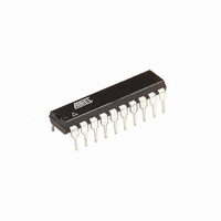
ATTINY26-16PI Atmel, ATTINY26-16PI Datasheet - Page 59

ATTINY26-16PI
Manufacturer Part Number
ATTINY26-16PI
Description
IC AVR MCU 2K 16MHZ IND 20-DIP
Manufacturer
Atmel
Series
AVR® ATtinyr
Specifications of ATTINY26-16PI
Core Processor
AVR
Core Size
8-Bit
Speed
16MHz
Connectivity
USI
Peripherals
Brown-out Detect/Reset, POR, PWM, WDT
Number Of I /o
16
Program Memory Size
2KB (1K x 16)
Program Memory Type
FLASH
Eeprom Size
128 x 8
Ram Size
128 x 8
Voltage - Supply (vcc/vdd)
4.5 V ~ 5.5 V
Data Converters
A/D 11x10b
Oscillator Type
Internal
Operating Temperature
-40°C ~ 85°C
Package / Case
20-DIP (0.300", 7.62mm)
Lead Free Status / RoHS Status
Contains lead / RoHS non-compliant
- Current page: 59 of 182
- Download datasheet (3Mb)
General Interrupt Flag
Register – GIFR
Timer/Counter
Interrupt Mask
Register – TIMSK
1477K–AVR–08/10
• Bit 5 – PCIE1: Pin Change Interrupt Enable1
When the PCIE1 bit is set (one) and the I-bit in the Status Register (SREG) is set (one), the
interrupt pin change is enabled on analog pins PB[7:4], PA[7:6] and PA[3]. Unless the alternate
function masks out the interrupt, any change on the pin mentioned before will cause an interrupt.
The corresponding interrupt of Pin Change Interrupt Request is executed from program memory
address $002. See also “Pin Change Interrupt” on page 62.
• Bit 4– PCIE0: Pin Change Interrupt Enable0
When the PCIE0 bit is set (one) and the I-bit in the Status Register (SREG) is set (one), the
interrupt pin change is enabled on digital pins PB[3:0]. Unless the alternate function masks out
the interrupt, any change on the pin mentioned before will cause an interrupt. The corresponding
interrupt of Pin Change Interrupt Request is executed from program memory address $002. See
also “Pin Change Interrupt” on page 62.
• Bits 3..0 – Res: Reserved Bits
These bits are reserved bits in the ATtiny26(L) and always read as zero.
• Bit 7 – Res: Reserved Bit
This bit is a reserved bit in the ATtiny26(L) and always reads as zero.
• Bit 6 – INTF0: External Interrupt Flag0
When an event on the INT0 pin triggers an interrupt request, INTF0 becomes set (one). If the I-
bit in SREG and the INT0 bit in GIMSK are set (one), the MCU will jump to the Interrupt Vector at
address $001. The flag is cleared when the interrupt routine is executed. Alternatively, the flag
can be cleared by writing a logical one to it. The flag is always cleared when INT0 is configured
as level interrupt.
• Bit 5 – PCIF: Pin Change Interrupt Flag
When an event on pins PB[7:0], PA[7:6], or PA[3] triggers an interrupt request, PCIF becomes
set (one). PCIE1 enables interrupt from analog pins PB[7:4], PA[7:6], and PA[3]. PCIE0 enables
interrupt on digital pins PB[3:0]. Note that pin change interrupt enable bits PCIE1 and PCIE0
also mask the flag if they are not set. For example, if PCIE0 is cleared, a pin change on PB[3:0]
does not set PCIF. If an alternate function is enabled on a pin, PCIF is masked from that individ-
ual pin. If the I-bit in SREG and the PCIE bit in GIMSK are set (one), the MCU will jump to the
Interrupt Vector at address $002. The flag is cleared when the interrupt routine is executed.
Alternatively, the flag can be cleared by writing a logical one to it. See also “Pin Change Inter-
rupt” on page 62.
• Bits 4..0 – Res: Reserved Bits
These bits are reserved bits in the ATtiny26(L) and always read as zero.
• Bit 7 – Res: Reserved Bit
This bit is a reserved bit in the ATtiny26(L) and always reads as zero.
Bit
$3A ($5A)
Read/Write
Initial Value
Bit
$39 ($59)
Read/Write
Initial Value
R
7
–
0
R
7
–
0
OCIE1A
INTF0
R/W
R/W
6
0
6
0
OCIE1B
PCIF
R/W
R/W
5
0
5
0
4
–
R
0
R
4
–
0
R
3
–
0
R
3
–
0
R
2
–
0
TOIE1
R/W
2
0
R
1
–
0
TOIE0
R/W
1
0
R
0
–
0
R
0
–
0
GIFR
TIMSK
59
Related parts for ATTINY26-16PI
Image
Part Number
Description
Manufacturer
Datasheet
Request
R

Part Number:
Description:
Manufacturer:
Atmel Corporation
Datasheet:

Part Number:
Description:
IC AVR MCU 2K 16MHZ IND 32-QFN
Manufacturer:
Atmel
Datasheet:

Part Number:
Description:
IC AVR MCU 2K 16MHZ IND 20-SOIC
Manufacturer:
Atmel
Datasheet:

Part Number:
Description:
IC AVR MCU 2K 16MHZ IND 20-DIP
Manufacturer:
Atmel
Datasheet:

Part Number:
Description:
IC AVR MCU 2K 16MHZ IND 32-QFN
Manufacturer:
Atmel
Datasheet:

Part Number:
Description:
IC AVR MCU 2K 16MHZ COM 20-SOIC
Manufacturer:
Atmel
Datasheet:

Part Number:
Description:
IC AVR MCU 2K 16MHZ IND 20-SOIC
Manufacturer:
Atmel
Datasheet:

Part Number:
Description:
ID MCU AVR 2K 5V 16MHZ 32-QFN
Manufacturer:
Atmel
Datasheet:

Part Number:
Description:
Microcontrollers (MCU) AVR 2K FLASH 128B EE 128B SRAM ADC
Manufacturer:
Atmel
Datasheet:

Part Number:
Description:
IC AVR MCU 2K 16MHZ COM 32-QFN
Manufacturer:
Atmel
Datasheet:

Part Number:
Description:
IC AVR MCU 2K 16MHZ COM 20-DIP
Manufacturer:
Atmel
Datasheet:

Part Number:
Description:
ID MCU AVR 2K 5V 16MHZ 20-DIP
Manufacturer:
Atmel
Datasheet:

Part Number:
Description:
ID MCU AVR 2K 5V 16MHZ 20-SOIC
Manufacturer:
Atmel
Datasheet:

Part Number:
Description:
IC MCU AVR 2K 16MHZ IND 20SOIC
Manufacturer:
Atmel
Datasheet:


