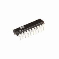
ATTINY26-16PI Atmel, ATTINY26-16PI Datasheet - Page 20

ATTINY26-16PI
Manufacturer Part Number
ATTINY26-16PI
Description
IC AVR MCU 2K 16MHZ IND 20-DIP
Manufacturer
Atmel
Series
AVR® ATtinyr
Specifications of ATTINY26-16PI
Core Processor
AVR
Core Size
8-Bit
Speed
16MHz
Connectivity
USI
Peripherals
Brown-out Detect/Reset, POR, PWM, WDT
Number Of I /o
16
Program Memory Size
2KB (1K x 16)
Program Memory Type
FLASH
Eeprom Size
128 x 8
Ram Size
128 x 8
Voltage - Supply (vcc/vdd)
4.5 V ~ 5.5 V
Data Converters
A/D 11x10b
Oscillator Type
Internal
Operating Temperature
-40°C ~ 85°C
Package / Case
20-DIP (0.300", 7.62mm)
Lead Free Status / RoHS Status
Contains lead / RoHS non-compliant
- Current page: 20 of 182
- Download datasheet (3Mb)
EEPROM Write During
Power-down Sleep
Mode
Preventing EEPROM
Corruption
I/O Memory
20
ATtiny26(L)
The EEPROM Read Enable Signal – EERE – is the read strobe to the EEPROM. When the cor-
rect address is set up in the EEAR Register, the EERE bit must be set. When the EERE bit is
cleared (zero) by hardware, requested data is found in the EEDR Register. The EEPROM read
access takes one instruction and there is no need to poll the EERE bit. When EERE has been
set, the CPU is halted for four cycles before the next instruction is executed.
The user should poll the EEWE bit before starting the read operation. If a write operation is in
progress when new data or address is written to the EEPROM I/O Registers, the write operation
will be interrupted, and the result is undefined.
Table 1. EEPROM Programming Time
Note:
When entering Power-down sleep mode while an EEPROM write operation is active, the
EEPROM write operation will continue, and will complete before the write access time has
passed. However, when the write operation is completed, the crystal Oscillator continues run-
ning, and as a consequence, the device does not enter Power-down entirely. It is therefore
recommended to verify that the EEPROM write operation is completed before entering Power-
down.
During periods of low V
too low for the CPU and the EEPROM to operate properly. These issues are the same as for
board level systems using the EEPROM, and the same design solutions should be applied.
An EEPROM data corruption can be caused by two situations when the voltage is too low. First,
a regular write sequence to the EEPROM requires a minimum voltage to operate correctly. Sec-
ondly, the CPU itself can execute instructions incorrectly, if the supply voltage for executing
instructions is too low.
EEPROM data corruption can easily be avoided by following these design recommendations
(one is sufficient):
1. Keep the AVR RESET active (low) during periods of insufficient power supply voltage.
2. Keep the AVR core in Power-down Sleep mode during periods of low V
Store constants in Flash memory if the ability to change memory contents from software is not
required. Flash memory can not be updated by the CPU, and will not be subject to corruption.
The I/O space definition of the ATtiny26(L) is shown in Table 2
Table 2. ATtiny26(L) I/O Space
Symbol
EEPROM Write (from CPU)
Address Hex
$3D ($5D)
$3F ($5F)
$3B ($5B)
This can be done by enabling the internal Brown-out Detector (BOD) if the operating volt-
age matches the detection level. If not, an external Brown-out Reset Protection circuit
can be applied.
vent the CPU from attempting to decode and execute instructions, effectively protecting
the EEPROM Registers from unintentional writes.
1. Uses 1 MHz clock, independent of CKSEL-Fuse settings.
GIMSK
SREG
Name
SP
CC,
the EEPROM data can be corrupted because the supply voltage is
Function
Status Register
Stack Pointer
General Interrupt Mask Register
Number of Calibrated RC
(1)
Oscillator Cycles
8448
(1)
Typical Programming
8.5 ms
Time
CC
. This will pre-
1477K–AVR–08/10
Related parts for ATTINY26-16PI
Image
Part Number
Description
Manufacturer
Datasheet
Request
R

Part Number:
Description:
Manufacturer:
Atmel Corporation
Datasheet:

Part Number:
Description:
IC AVR MCU 2K 16MHZ IND 32-QFN
Manufacturer:
Atmel
Datasheet:

Part Number:
Description:
IC AVR MCU 2K 16MHZ IND 20-SOIC
Manufacturer:
Atmel
Datasheet:

Part Number:
Description:
IC AVR MCU 2K 16MHZ IND 20-DIP
Manufacturer:
Atmel
Datasheet:

Part Number:
Description:
IC AVR MCU 2K 16MHZ IND 32-QFN
Manufacturer:
Atmel
Datasheet:

Part Number:
Description:
IC AVR MCU 2K 16MHZ COM 20-SOIC
Manufacturer:
Atmel
Datasheet:

Part Number:
Description:
IC AVR MCU 2K 16MHZ IND 20-SOIC
Manufacturer:
Atmel
Datasheet:

Part Number:
Description:
ID MCU AVR 2K 5V 16MHZ 32-QFN
Manufacturer:
Atmel
Datasheet:

Part Number:
Description:
Microcontrollers (MCU) AVR 2K FLASH 128B EE 128B SRAM ADC
Manufacturer:
Atmel
Datasheet:

Part Number:
Description:
IC AVR MCU 2K 16MHZ COM 32-QFN
Manufacturer:
Atmel
Datasheet:

Part Number:
Description:
IC AVR MCU 2K 16MHZ COM 20-DIP
Manufacturer:
Atmel
Datasheet:

Part Number:
Description:
ID MCU AVR 2K 5V 16MHZ 20-DIP
Manufacturer:
Atmel
Datasheet:

Part Number:
Description:
ID MCU AVR 2K 5V 16MHZ 20-SOIC
Manufacturer:
Atmel
Datasheet:

Part Number:
Description:
IC MCU AVR 2K 16MHZ IND 20SOIC
Manufacturer:
Atmel
Datasheet:


