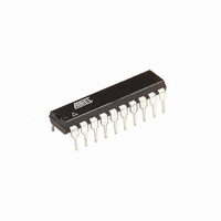
ATTINY26-16PI Atmel, ATTINY26-16PI Datasheet - Page 54

ATTINY26-16PI
Manufacturer Part Number
ATTINY26-16PI
Description
IC AVR MCU 2K 16MHZ IND 20-DIP
Manufacturer
Atmel
Series
AVR® ATtinyr
Specifications of ATTINY26-16PI
Core Processor
AVR
Core Size
8-Bit
Speed
16MHz
Connectivity
USI
Peripherals
Brown-out Detect/Reset, POR, PWM, WDT
Number Of I /o
16
Program Memory Size
2KB (1K x 16)
Program Memory Type
FLASH
Eeprom Size
128 x 8
Ram Size
128 x 8
Voltage - Supply (vcc/vdd)
4.5 V ~ 5.5 V
Data Converters
A/D 11x10b
Oscillator Type
Internal
Operating Temperature
-40°C ~ 85°C
Package / Case
20-DIP (0.300", 7.62mm)
Lead Free Status / RoHS Status
Contains lead / RoHS non-compliant
- Current page: 54 of 182
- Download datasheet (3Mb)
Table 27. Overriding Signals for Alternate Functions in PB7..PB4
Notes:
54
Signal
Name
PUOE
PUOV
DDOE
DDOV
PVOE
PVOV
DIEOE
DIEOV
DI
AIO
1. RSTDISBL Fuse (active low) is described in section “System Control and Reset” on page 32.
2. Note that the PCINT1 Interrupt is only enabled if both the Global Interrupt Flag is enabled, the PCIE1 flag in GIMSK is set
3. PB5IOENABLE and PB4IOENABLE are given by the PLLCK and CKSEL Fuses as described in “Clock Sources” on page
4. External low level interrupt is enabled if both the Global Interrupt Flag is enabled and the INT0 flag in GIMSK is set as
5. Not operator is marked with “~”.
6. The operation of the Timer/Counter0 with external clock disabled is described in “8-bit Timer/Counter0” on page 65.
7. External clock is selected by the PLLCK and CKSEL Fuses as described in “Clock Sources” on page 25.
ATtiny26(L)
and the alternate function of the pin is disabled as described in “Pin Change Interrupt” on page 62.
25.
described in “External Interrupt” on page 62.
PB7/ADC10/RESET/
PCINT1
RSTDSBL
1
RSTDSBL
0
0
0
PCINT1_ENABLE
PCINT1_ENABLE
~
PCINT1
ADC10, RESET INPUT
(5)
RSTDSBL
(1)
(1)
(1)
• DI/SDA/OC1A/PCINT0 – Port B, Bit 0
DI: Data Input in USI Three-wire mode. USI Three-wire mode does not override normal port
functions., so pin must be configure as an input.
SDA: Serial Data in USI Two-wire mode. Serial data pin is bi-directional and uses open-collector
output. The SDA pin is enabled by setting the pin as an output. The pin is pulled low when the
PORTB0 or USI shiftRegister is zero when DDB0 is set (one). Pull-up is disabled in USI Two-
wire mode.
OC1A: Inverted Timer/Counter1 PWM output A: The PB0 pin can serve as an Inverted output for
the PWM mode if not used in programming or USI. The PB0 pin has to be configured as an out-
put (DDB0 set (one)) to serve this function.
PCINT0: Pin Change Interrupt 0 pin. Pin change interrupt is enabled on pin when global interrupt
is enabled, pin change interrupt is enabled and the alternate functions do not mask the interrupt.
The masking alternate functions are the inverted output compare match output OC1A and USI
data DI or SDA. Digital input is enabled on pin PB0 also in SLEEP modes, if the pin change
interrupt is enabled and not masked by the alternate functions. Table 27 and Table 28 relate the
alternate functions of Port B to the overriding signals shown in “Alternate Port Functions” on
page 46.
(2)
(2)
| RSTDSBL
•
(1)
PB6/ADC9/INT0/TO/
PCINT1
0
0
0
0
0
0
~T0_EXT_CLOCK
PCINT1_ENABLE
INT0_ENABLE
1
INT0, T0, PCINT1
ADC9
(4)
(2)
(6)
|
•
PB5/ADC8/XTAL2/
PCINT1
~
0
~PB5IOENABLE
0
0
0
PCINT1_ENABLE
~PB5IOENABLE
PCINT1_ENABLE
PB5IOENABLE
PCINT1
ADC8, XTAL2
(5)
PB5IOENABLE
(3)
(3)
(3)
(2)
(2)
(3)
|
•
PB4/ADC7/XTAL1
~PB4IOENABLE
0
~PB4IOENABLE
0
0
0
PCINT_ ENABLE
~PB4IOENABLE
EXT_CLOCK_ENABLE
PCINT1_ENABLE
PB4IOENABLE
EXT_CLOCK_ENABLE
External Clock, PCINT1
XTAL1
1477K–AVR–08/10
(3)
(3)
(3)
(3)
|
(2)
(2)
|
•
|
(7)
Related parts for ATTINY26-16PI
Image
Part Number
Description
Manufacturer
Datasheet
Request
R

Part Number:
Description:
Manufacturer:
Atmel Corporation
Datasheet:

Part Number:
Description:
IC AVR MCU 2K 16MHZ IND 32-QFN
Manufacturer:
Atmel
Datasheet:

Part Number:
Description:
IC AVR MCU 2K 16MHZ IND 20-SOIC
Manufacturer:
Atmel
Datasheet:

Part Number:
Description:
IC AVR MCU 2K 16MHZ IND 20-DIP
Manufacturer:
Atmel
Datasheet:

Part Number:
Description:
IC AVR MCU 2K 16MHZ IND 32-QFN
Manufacturer:
Atmel
Datasheet:

Part Number:
Description:
IC AVR MCU 2K 16MHZ COM 20-SOIC
Manufacturer:
Atmel
Datasheet:

Part Number:
Description:
IC AVR MCU 2K 16MHZ IND 20-SOIC
Manufacturer:
Atmel
Datasheet:

Part Number:
Description:
ID MCU AVR 2K 5V 16MHZ 32-QFN
Manufacturer:
Atmel
Datasheet:

Part Number:
Description:
Microcontrollers (MCU) AVR 2K FLASH 128B EE 128B SRAM ADC
Manufacturer:
Atmel
Datasheet:

Part Number:
Description:
IC AVR MCU 2K 16MHZ COM 32-QFN
Manufacturer:
Atmel
Datasheet:

Part Number:
Description:
IC AVR MCU 2K 16MHZ COM 20-DIP
Manufacturer:
Atmel
Datasheet:

Part Number:
Description:
ID MCU AVR 2K 5V 16MHZ 20-DIP
Manufacturer:
Atmel
Datasheet:

Part Number:
Description:
ID MCU AVR 2K 5V 16MHZ 20-SOIC
Manufacturer:
Atmel
Datasheet:

Part Number:
Description:
IC MCU AVR 2K 16MHZ IND 20SOIC
Manufacturer:
Atmel
Datasheet:


