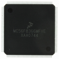
MC56F8366MFVE Freescale Semiconductor, MC56F8366MFVE Datasheet - Page 136

MC56F8366MFVE
Manufacturer Part Number
MC56F8366MFVE
Description
IC DSP 16BIT 60MHZ 144-LQFP
Manufacturer
Freescale Semiconductor
Series
56F8xxxr
Datasheet
1.MC56F8366VFVE.pdf
(182 pages)
Specifications of MC56F8366MFVE
Core Processor
56800
Core Size
16-Bit
Speed
60MHz
Connectivity
CAN, EBI/EMI, SCI, SPI
Peripherals
POR, PWM, Temp Sensor, WDT
Number Of I /o
62
Program Memory Size
544KB (272K x 16)
Program Memory Type
FLASH
Ram Size
18K x 16
Voltage - Supply (vcc/vdd)
2.25 V ~ 3.6 V
Data Converters
A/D 16x12b
Oscillator Type
External
Operating Temperature
-40°C ~ 125°C
Package / Case
144-LQFP
For Use With
MC56F8367EVME - EVAL BOARD FOR MC56F83X
Lead Free Status / RoHS Status
Lead free / RoHS Compliant
Eeprom Size
-
Available stocks
Company
Part Number
Manufacturer
Quantity
Price
Company:
Part Number:
MC56F8366MFVE
Manufacturer:
Freescale
Quantity:
440
Company:
Part Number:
MC56F8366MFVE
Manufacturer:
Freescale Semiconductor
Quantity:
10 000
Part Number:
MC56F8366MFVE
Manufacturer:
FREESCALE
Quantity:
20 000
- Current page: 136 of 182
- Download datasheet (2Mb)
Two examples of FM_CLKDIV calculations follow.
EXAMPLE 1: If the system clock is the 8MHz crystal frequency because the PLL has not been set up,
the input clock will be below 12.8MHz, so PRDIV8 = FM_CLKDIV[6] = 0. Using the following equation
yields a DIV value of 19 for a clock of 200kHz, and a DIV value of 20 for a clock of 190kHz. This
translates into an FM_CLKDIV[6:0] value of $13 or $14, respectively.
EXAMPLE 2: In this example, the system clock has been set up with a value of 32MHz, making the FM
input clock 16MHz. Because that is greater than 12.8MHz, PRDIV8 = FM_CLKDIV[6] = 1. Using the
following equation yields a DIV value of 9 for a clock of 200kHz, and a DIV value of 10 for a clock of
181kHz. This translates to an FM_CLKDIV[6:0] value of $49 or $4A, respectively.
Once the LOCKOUT_RECOVERY instruction has been shifted into the instruction register, the clock
divider value must be shifted into the corresponding 7-bit data register. After the data register has been
updated, the user must transition the TAP controller into the RUN-TEST/IDLE state for the lockout
sequence to commence. The controller must remain in this state until the erase sequence has completed.
For details, see the JTAG Section in the 56F8300 Peripheral User Manual.
Note:
136
Once the lockout recovery sequence has completed, the user must reset both the JTAG TAP controller
(by asserting TRST) and the device (by asserting external chip reset) to return to normal unsecured
operation.
JTAG
SYS_CLK
Figure 7-1 JTAG to FM Connection for Lockout Recovery
2
FM_CLKDIV
FM_ERASE
150[kHz]
150[kHz]
56F8366 Technical Data, Rev. 7
<
<
(
(
FMCLKD
clock
input
SYS_CLK
SYS_CLK
(DIV + 1)
(DIV + 1)
(2)(8)
(2)
7
)
)
Flash Memory
<
<
7
200[kHz]
200[kHz]
DIVIDER
7
Freescale Semiconductor
Preliminary
Related parts for MC56F8366MFVE
Image
Part Number
Description
Manufacturer
Datasheet
Request
R
Part Number:
Description:
56f8300 16-bit Digital Signal Controllers
Manufacturer:
Freescale Semiconductor, Inc
Datasheet:
Part Number:
Description:
Manufacturer:
Freescale Semiconductor, Inc
Datasheet:
Part Number:
Description:
Manufacturer:
Freescale Semiconductor, Inc
Datasheet:
Part Number:
Description:
Manufacturer:
Freescale Semiconductor, Inc
Datasheet:
Part Number:
Description:
Manufacturer:
Freescale Semiconductor, Inc
Datasheet:
Part Number:
Description:
Manufacturer:
Freescale Semiconductor, Inc
Datasheet:
Part Number:
Description:
Manufacturer:
Freescale Semiconductor, Inc
Datasheet:
Part Number:
Description:
Manufacturer:
Freescale Semiconductor, Inc
Datasheet:
Part Number:
Description:
Manufacturer:
Freescale Semiconductor, Inc
Datasheet:
Part Number:
Description:
Manufacturer:
Freescale Semiconductor, Inc
Datasheet:
Part Number:
Description:
Manufacturer:
Freescale Semiconductor, Inc
Datasheet:
Part Number:
Description:
Manufacturer:
Freescale Semiconductor, Inc
Datasheet:
Part Number:
Description:
Manufacturer:
Freescale Semiconductor, Inc
Datasheet:
Part Number:
Description:
Manufacturer:
Freescale Semiconductor, Inc
Datasheet:
Part Number:
Description:
Manufacturer:
Freescale Semiconductor, Inc
Datasheet:


