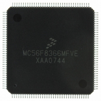
MC56F8366MFVE Freescale Semiconductor, MC56F8366MFVE Datasheet - Page 124

MC56F8366MFVE
Manufacturer Part Number
MC56F8366MFVE
Description
IC DSP 16BIT 60MHZ 144-LQFP
Manufacturer
Freescale Semiconductor
Series
56F8xxxr
Datasheet
1.MC56F8366VFVE.pdf
(182 pages)
Specifications of MC56F8366MFVE
Core Processor
56800
Core Size
16-Bit
Speed
60MHz
Connectivity
CAN, EBI/EMI, SCI, SPI
Peripherals
POR, PWM, Temp Sensor, WDT
Number Of I /o
62
Program Memory Size
544KB (272K x 16)
Program Memory Type
FLASH
Ram Size
18K x 16
Voltage - Supply (vcc/vdd)
2.25 V ~ 3.6 V
Data Converters
A/D 16x12b
Oscillator Type
External
Operating Temperature
-40°C ~ 125°C
Package / Case
144-LQFP
For Use With
MC56F8367EVME - EVAL BOARD FOR MC56F83X
Lead Free Status / RoHS Status
Lead free / RoHS Compliant
Eeprom Size
-
Available stocks
Company
Part Number
Manufacturer
Quantity
Price
Company:
Part Number:
MC56F8366MFVE
Manufacturer:
Freescale
Quantity:
440
Company:
Part Number:
MC56F8366MFVE
Manufacturer:
Freescale Semiconductor
Quantity:
10 000
Part Number:
MC56F8366MFVE
Manufacturer:
FREESCALE
Quantity:
20 000
6.5.7.6
6.5.7.7
Selects clock to be muxed out on the CLKO pin.
6.5.8
Some GPIO pads can have more than one peripheral selected as the alternate function instead of GPIO.
For these pads, this register selects which of the alternate peripherals are actually selected for the GPIO
peripheral function. This applies to GPIOC, pins 0-3, and to GPIOD, pins 0 and 1.
The GPIOC Peripheral Select register can be used to multiplex out any one of the three alternate
peripherals for GPIOC. The default peripheral is Quad Decoder 1 and Quad Timer B (NOT available in
the 56F8166 device); these peripherals work together.
The four I/O pins associated with GPIOC can function as GPIO, Quad Decoder 1/Quad Timer B, or as
SPI 1 signals. GPIO is not the default and is enabled/disabled via the GPIOC_PER, as shown in
Figure 6-10
choice between decoder/timer and SPI inputs/outputs is made in the SIM_GPS register and in conjunction
with the Quad Timer Status and Control Registers (SCR). The default state is for the peripheral function
of GPIOC[3:0] to be programmed as decoder functions. This can be changed by altering the appropriate
controls in the indicated registers.
124
•
•
•
•
•
•
•
•
•
•
•
•
•
•
•
•
•
•
•
•
0 = CLKOUT output is enabled and will output the signal indicated by CLKOSEL
1 = CLKOUT is tri-stated
00000 = SYS_CLK (from OCCS - DEFAULT)
00001 = Reserved for factory test—56800E clock
00010 = Reserved for factory test—XRAM clock
00011 = Reserved for factory test—PFLASH odd clock
00100 = Reserved for factory test—PFLASH even clock
00101 = Reserved for factory test—BFLASH clock
00110 = Reserved for factory test—DFLASH clock
00111 = Oscillator output
01000 = F
01001 = Reserved for factory test—IPB clock
01010 = Reserved for factory test—Feedback (from OCCS, this is path to PLL)
01011 = Reserved for factory test—Prescaler clock (from OCCS)
01100 = Reserved for factory test—Postscaler clock (from OCCS)
01101 = Reserved for factory test—SYS_CLK2 (from OCCS)
01110 = Reserved for factory test—SYS_CLK_DIV2
01111 = Reserved for factory test—SYS_CLK_D
10000 = ADCA clock
10001 = ADCB clock
GPIO Peripheral Select Register (SIM_GPS)
Clockout Disable (CLKDIS)—Bit 5
CLockout Select (CLKOSEL)—Bits 4–0
and
out
Table
(from OCCS)
6-2. When GPIOC[3:0] are programmed to operate as peripheral I/O, then the
56F8366 Technical Data, Rev. 7
Freescale Semiconductor
Preliminary


