DF2378RVFQ34V Renesas Electronics America, DF2378RVFQ34V Datasheet - Page 232
DF2378RVFQ34V
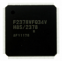
Manufacturer Part Number
DF2378RVFQ34V
Description
IC H8S MCU FLASH 512K 144LQFP
Manufacturer
Renesas Electronics America
Series
H8® H8S/2300r
Specifications of DF2378RVFQ34V
Core Processor
H8S/2000
Core Size
16-Bit
Speed
34MHz
Connectivity
I²C, IrDA, SCI, SmartCard
Peripherals
DMA, POR, PWM, WDT
Number Of I /o
97
Program Memory Size
512KB (512K x 8)
Program Memory Type
FLASH
Ram Size
32K x 8
Voltage - Supply (vcc/vdd)
3 V ~ 3.6 V
Data Converters
A/D 16x10b; D/A 6x8b
Oscillator Type
Internal
Operating Temperature
-20°C ~ 75°C
Package / Case
144-LQFP
For Use With
YLCDRSK2378 - KIT DEV EVAL H8S/2378 LCDYR0K42378FC000BA - KIT EVAL FOR H8S/2378HS0005KCU11H - EMULATOR E10A-USB H8S(X),SH2(A)EDK2378 - DEV EVAL KIT FOR H8S/2378
Lead Free Status / RoHS Status
Lead free / RoHS Compliant
Eeprom Size
-
Available stocks
Company
Part Number
Manufacturer
Quantity
Price
Company:

Part Number:
DF2378RVFQ34V
Manufacturer:
Renesas Electronics America
Quantity:
10 000


Section 6 Bus Controller (BSC)
6.3.9
DRACCR is used to set the DRAM/synchronous DRAM interface bus specifications.
Note: The synchronous DRAM interface is not supported by the H8S/2378 Group.
Bit
15
14
13
12
11
Rev.7.00 Mar. 18, 2009 page 164 of 1136
REJ09B0109-0700
Bit Name
DRMI
—
TPC1
TPC0
SDWCD
DRAM Access Control Register (DRACCR)
Initial Value
0
0
0
0
0 *
R/W
R/W
R/W
R/W
R/W
R/W
Description
Idle Cycle Insertion
An idle cycle can be inserted after a
DRAM/synchronous DRAM access cycle when a
continuous normal space access cycle follows a
DRAM/synchronous DRAM access cycle. Idle cycle
insertion conditions, setting of number of states,
etc., comply with settings of bits ICIS2, ICIS1,
ICIS0, and IDLC in BCR register
0: Idle cycle not inserted
1: Idle cycle inserted
Reserved
This bit can be read from or written to. However,
the write value should always be 0.
Precharge State Control
These bits select the number of states in the RAS
precharge cycle in normal access and refreshing.
00: 1 state
01: 2 states
10: 3 states
11: 4 states
CAS Latency Control Cycle Disabled during
Continuous Synchronous DRAM Space Write
Access
Disables CAS latency control cycle (Tcl) inserted
by WTCRB (H) settings during synchronous DRAM
write access (see figure 6.5).
0: Enables CAS latency control cycle
1: Disables CAS latency control cycle
Related parts for DF2378RVFQ34V
Image
Part Number
Description
Manufacturer
Datasheet
Request
R

Part Number:
Description:
KIT STARTER FOR M16C/29
Manufacturer:
Renesas Electronics America
Datasheet:

Part Number:
Description:
KIT STARTER FOR R8C/2D
Manufacturer:
Renesas Electronics America
Datasheet:

Part Number:
Description:
R0K33062P STARTER KIT
Manufacturer:
Renesas Electronics America
Datasheet:

Part Number:
Description:
KIT STARTER FOR R8C/23 E8A
Manufacturer:
Renesas Electronics America
Datasheet:

Part Number:
Description:
KIT STARTER FOR R8C/25
Manufacturer:
Renesas Electronics America
Datasheet:

Part Number:
Description:
KIT STARTER H8S2456 SHARPE DSPLY
Manufacturer:
Renesas Electronics America
Datasheet:

Part Number:
Description:
KIT STARTER FOR R8C38C
Manufacturer:
Renesas Electronics America
Datasheet:

Part Number:
Description:
KIT STARTER FOR R8C35C
Manufacturer:
Renesas Electronics America
Datasheet:

Part Number:
Description:
KIT STARTER FOR R8CL3AC+LCD APPS
Manufacturer:
Renesas Electronics America
Datasheet:
Part Number:
Description:
KIT STARTER FOR RX610
Manufacturer:
Renesas Electronics America
Datasheet:

Part Number:
Description:
KIT STARTER FOR R32C/118
Manufacturer:
Renesas Electronics America
Datasheet:

Part Number:
Description:
KIT DEV RSK-R8C/26-29
Manufacturer:
Renesas Electronics America
Datasheet:

Part Number:
Description:
KIT STARTER FOR SH7124
Manufacturer:
Renesas Electronics America
Datasheet:

Part Number:
Description:
KIT STARTER FOR H8SX/1622
Manufacturer:
Renesas Electronics America
Datasheet:

Part Number:
Description:
KIT DEV FOR SH7203
Manufacturer:
Renesas Electronics America
Datasheet: