DF2378RVFQ34V Renesas Electronics America, DF2378RVFQ34V Datasheet - Page 1049
DF2378RVFQ34V
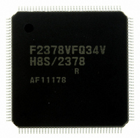
Manufacturer Part Number
DF2378RVFQ34V
Description
IC H8S MCU FLASH 512K 144LQFP
Manufacturer
Renesas Electronics America
Series
H8® H8S/2300r
Specifications of DF2378RVFQ34V
Core Processor
H8S/2000
Core Size
16-Bit
Speed
34MHz
Connectivity
I²C, IrDA, SCI, SmartCard
Peripherals
DMA, POR, PWM, WDT
Number Of I /o
97
Program Memory Size
512KB (512K x 8)
Program Memory Type
FLASH
Ram Size
32K x 8
Voltage - Supply (vcc/vdd)
3 V ~ 3.6 V
Data Converters
A/D 16x10b; D/A 6x8b
Oscillator Type
Internal
Operating Temperature
-20°C ~ 75°C
Package / Case
144-LQFP
For Use With
YLCDRSK2378 - KIT DEV EVAL H8S/2378 LCDYR0K42378FC000BA - KIT EVAL FOR H8S/2378HS0005KCU11H - EMULATOR E10A-USB H8S(X),SH2(A)EDK2378 - DEV EVAL KIT FOR H8S/2378
Lead Free Status / RoHS Status
Lead free / RoHS Compliant
Eeprom Size
-
Available stocks
Company
Part Number
Manufacturer
Quantity
Price
Company:

Part Number:
DF2378RVFQ34V
Manufacturer:
Renesas Electronics America
Quantity:
10 000


The address list gives information on the on-chip I/O register addresses, how the register bits are
configured, and the register states in each operating mode. The information is given as shown
below.
1. Register addresses (address order)
• Registers are listed from the lower allocation addresses.
• Reserved addresses are indicated by ⎯ in the register name column. Do not access to reserved
• For the addresses of 16 or 32 bits, the MSB-side address is described.
• Registers are classified by functional modules.
• The access size is indicated.
2. Register bits
• Bit configurations of the registers are described in the same order as the register addresses.
• Reserved bits are indicated by ⎯ in the bit name column.
• For the registers of 16 or 32 bits, the MSB is described first.
3. Register states in each operating mode
• Register states are described in the same order as the register addresses.
• The register states described here are for the basic operating modes. If there is a specific reset
25.1
The data bus width indicates the numbers of bits by which the register is accessed.
The number of access states indicates the number of states based on the specified reference clock.
addresses.
for an on-chip peripheral module, refer to the section on that on-chip peripheral module.
Register Addresses (Address Order)
Section 25 List of Registers
Rev.7.00 Mar. 18, 2009 page 981 of 1136
Section 25 List of Registers
REJ09B0109-0700
Related parts for DF2378RVFQ34V
Image
Part Number
Description
Manufacturer
Datasheet
Request
R

Part Number:
Description:
KIT STARTER FOR M16C/29
Manufacturer:
Renesas Electronics America
Datasheet:

Part Number:
Description:
KIT STARTER FOR R8C/2D
Manufacturer:
Renesas Electronics America
Datasheet:

Part Number:
Description:
R0K33062P STARTER KIT
Manufacturer:
Renesas Electronics America
Datasheet:

Part Number:
Description:
KIT STARTER FOR R8C/23 E8A
Manufacturer:
Renesas Electronics America
Datasheet:

Part Number:
Description:
KIT STARTER FOR R8C/25
Manufacturer:
Renesas Electronics America
Datasheet:

Part Number:
Description:
KIT STARTER H8S2456 SHARPE DSPLY
Manufacturer:
Renesas Electronics America
Datasheet:

Part Number:
Description:
KIT STARTER FOR R8C38C
Manufacturer:
Renesas Electronics America
Datasheet:

Part Number:
Description:
KIT STARTER FOR R8C35C
Manufacturer:
Renesas Electronics America
Datasheet:

Part Number:
Description:
KIT STARTER FOR R8CL3AC+LCD APPS
Manufacturer:
Renesas Electronics America
Datasheet:
Part Number:
Description:
KIT STARTER FOR RX610
Manufacturer:
Renesas Electronics America
Datasheet:

Part Number:
Description:
KIT STARTER FOR R32C/118
Manufacturer:
Renesas Electronics America
Datasheet:

Part Number:
Description:
KIT DEV RSK-R8C/26-29
Manufacturer:
Renesas Electronics America
Datasheet:

Part Number:
Description:
KIT STARTER FOR SH7124
Manufacturer:
Renesas Electronics America
Datasheet:

Part Number:
Description:
KIT STARTER FOR H8SX/1622
Manufacturer:
Renesas Electronics America
Datasheet:

Part Number:
Description:
KIT DEV FOR SH7203
Manufacturer:
Renesas Electronics America
Datasheet: