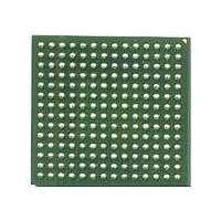
MCF5272VM66J Freescale Semiconductor, MCF5272VM66J Datasheet - Page 308

MCF5272VM66J
Manufacturer Part Number
MCF5272VM66J
Description
IC MCU 166MHZ 196MAPBGA
Manufacturer
Freescale Semiconductor
Series
MCF527xr
Datasheets
1.MCF5272CVF66J.pdf
(544 pages)
2.MCF5272CVF66J.pdf
(12 pages)
3.MCF5272VM66J.pdf
(44 pages)
Specifications of MCF5272VM66J
Core Processor
Coldfire V2
Core Size
32-Bit
Speed
66MHz
Connectivity
EBI/EMI, Ethernet, I²C, SPI, UART/USART, USB
Peripherals
DMA, WDT
Number Of I /o
32
Program Memory Size
16KB (4K x 32)
Program Memory Type
ROM
Ram Size
1K x 32
Voltage - Supply (vcc/vdd)
3 V ~ 3.6 V
Oscillator Type
External
Operating Temperature
0°C ~ 70°C
Package / Case
196-MAPBGA
Processor Series
MCF527x
Core
ColdFire V2
Data Bus Width
32 bit
Data Ram Size
64 KB
Interface Type
I2C, UART, Ethernet, SPI, USB, QSPI
Maximum Clock Frequency
166 MHz
Number Of Timers
4
Operating Supply Voltage
1.4 V to 1.6 V
Maximum Operating Temperature
+ 85 C
Mounting Style
SMD/SMT
3rd Party Development Tools
JLINK-CF-BDM26, EWCF
Development Tools By Supplier
NNDK-MOD5272-KIT, NNDK-MOD5270-KIT
Minimum Operating Temperature
- 40 C
Lead Free Status / RoHS Status
Lead free / RoHS Compliant
Eeprom Size
-
Data Converters
-
Lead Free Status / Rohs Status
Lead free / RoHS Compliant
Available stocks
Company
Part Number
Manufacturer
Quantity
Price
Company:
Part Number:
MCF5272VM66J
Manufacturer:
FREESCAL
Quantity:
416
Company:
Part Number:
MCF5272VM66J
Manufacturer:
Freescale
Quantity:
178
Company:
Part Number:
MCF5272VM66J
Manufacturer:
Freescale Semiconductor
Quantity:
10 000
- Current page: 308 of 544
- Download datasheet (7Mb)
Physical Layer Interface Controller (PLIC)
The above settings can be made by a single write of the 16-bit value 0x802B to PCSR.
The following restrictions should be observed when using the clock generator module:
Figure 13-11
PLIC block.
13-12
•
•
The smallest multiplication factor is 2.
CLKIN should be significantly greater than (> 20 times) the synthesized clock.
DCL0/URT1_CLK
PA8/FSC0/FSR0
GCI/IDL
GCI/IDL
GCI/IDL
GCI/IDL
Port 1
Port 2
Port 3
Port 0
and
O192K
P1CR[FSM]
Figure 13-12
FSC0
FSC1
MCF5272 ColdFire
DCL0
DFSC0
DCL1
FSC1
DCL1
DFSC2
DCL1
DFSC3
CKI[1:0]
Mux
Figure 13-11. PLIC Internal Timing Signal Routing
show the connectivity and relationship of the timing signals within the
DFSC0
Figure 13-12. PLIC Clock Generator
®
Prog Delay 0
Integrated Microprocessor User’s Manual, Rev. 3
P0SDR[15:0]
P1SDR[15:0]
P2SDR[15:0]
P3SDR[15:0]
CMULT[2:0]
Multiply
Prog Delay 1
Prog Delay 2
Block
Prog Delay 3
SFSC Gen
P0CR[M2-M0]
DFSC1
P1CR[M/S]
Pin
Mux 1
Pin
Mux 0
2-KHz to CPU
FDIV[2:0]
Divider
Block
DCL0/URT1_CLK
PA8/FSC0/FSR0
DCL1/GDCL1_OUT
FSC1/FSR1/DFSC1
DFSC2
DFSC3
Freescale Semiconductor
GDCL
Gen_FSC
Related parts for MCF5272VM66J
Image
Part Number
Description
Manufacturer
Datasheet
Request
R
Part Number:
Description:
Mcf5272 Coldfire Integrated Microprocessor User
Manufacturer:
Freescale Semiconductor, Inc
Datasheet:

Part Number:
Description:
MCF5272 Interrupt Service Routine for the Physical Layer Interface Controller
Manufacturer:
Freescale Semiconductor / Motorola
Datasheet:
Part Number:
Description:
Manufacturer:
Freescale Semiconductor, Inc
Datasheet:
Part Number:
Description:
Manufacturer:
Freescale Semiconductor, Inc
Datasheet:
Part Number:
Description:
Manufacturer:
Freescale Semiconductor, Inc
Datasheet:
Part Number:
Description:
Manufacturer:
Freescale Semiconductor, Inc
Datasheet:
Part Number:
Description:
Manufacturer:
Freescale Semiconductor, Inc
Datasheet:
Part Number:
Description:
Manufacturer:
Freescale Semiconductor, Inc
Datasheet:
Part Number:
Description:
Manufacturer:
Freescale Semiconductor, Inc
Datasheet:
Part Number:
Description:
Manufacturer:
Freescale Semiconductor, Inc
Datasheet:
Part Number:
Description:
Manufacturer:
Freescale Semiconductor, Inc
Datasheet:
Part Number:
Description:
Manufacturer:
Freescale Semiconductor, Inc
Datasheet:
Part Number:
Description:
Manufacturer:
Freescale Semiconductor, Inc
Datasheet:
Part Number:
Description:
Manufacturer:
Freescale Semiconductor, Inc
Datasheet:
Part Number:
Description:
Manufacturer:
Freescale Semiconductor, Inc
Datasheet:


