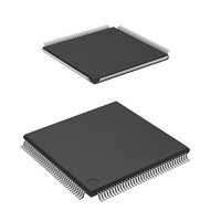
DF2160BVTE10 Renesas Electronics America, DF2160BVTE10 Datasheet - Page 601

DF2160BVTE10
Manufacturer Part Number
DF2160BVTE10
Description
IC H8S MCU FLASH 64K 144TQFP
Manufacturer
Renesas Electronics America
Series
H8® H8S/2100r
Datasheet
1.DF2160BVT10V.pdf
(847 pages)
Specifications of DF2160BVTE10
Core Processor
H8S/2000
Core Size
16-Bit
Speed
10MHz
Connectivity
Host Interface (LPC), I²C, IrDA, SCI, X-Bus
Peripherals
PWM, WDT
Number Of I /o
114
Program Memory Size
64KB (64K x 8)
Program Memory Type
FLASH
Ram Size
4K x 8
Voltage - Supply (vcc/vdd)
2.7 V ~ 3.6 V
Data Converters
A/D 8x10b; D/A 2x8b
Oscillator Type
Internal
Operating Temperature
-20°C ~ 75°C
Package / Case
144-TQFP, 144-VQFP
Lead Free Status / RoHS Status
Contains lead / RoHS non-compliant
Eeprom Size
-
Other names
HD64F2160BVTE10
HD64F2160BVTE10
HD64F2160BVTE10
- Current page: 601 of 847
- Download datasheet (5Mb)
19.3.5
The ODR registers are 8-bit readable/writable registers for the slave processor (this LSI), and 8-bit
read-only registers for the host processor. The registers selected from the host according to the I/O
address are shown in the following table. For information on ODR3 selection, see section 19.3.3,
LPC Channel 3 Address Register (LADR3). In an LPC I/O read cycle, the data in the selected
register is transferred to the host. The initial values of ODR1 to ODR3 are undefined.
19.3.6
The TWR registers are sixteen 8-bit readable/writable registers to both the slave processor (this
LSI) and the host processor. In TWR0, however, two registers (TWR0MW and TWR0SW) are
allocated to the same address for both the host address and the slave address. TWR0MW is a
write-only register for the host processor, and a read-only register for the slave processor, while
TWR0SW is a write-only register for the slave processor and a read-only register for the host
processor. When the host and slave processors begin a write, after the respective TWR0 registers
have been written to, access right arbitration for simultaneous access is performed by checking the
status flags to see if those writes were valid. For the registers selected from the host according to
the I/O address, see section 19.3.3, LPC Channel 3 Address Register (LADR3).
Data transferred in an LPC I/O write cycle is written to the selected register; in an LPC I/O read
cycle, the data in the selected register is transferred to the host. The initial values of TWR0 to
TWR15 are undefined.
19.3.7
The STR registers are 8-bit registers that indicate status information during host interface
processing. Bits 3, 1, and 0 of STR1 to STR3, and bits 7 to 4 of STR3, are read-only bits for both
the host processor and the slave processor (this LSI). However, only 0 can be written to bit 0 of
STR1 to STR3 and bits 6 and 4 of STR3, from the slave processor (this LSI), in order to clear the
flags to 0. The registers selected from the host processor according to the I/O address are shown in
the following table. For information on STR3 selection, see section 19.3.3, LPC Channel 3
Address Register (LADR3). In an LPC I/O read cycle, the data in the selected register is
transferred to the host processor. The initial values of STR1 to STR3 are H'00.
Bits 15 to 4
0000 0000 0110
0000 0000 0110
Output Data Registers 1 to 3 (ODR1 to ODR3)
Bidirectional Data Registers 0 to 15 (TWR0 to TWR15)
Status Registers 1 to 3 (STR1 to STR3)
I/O Address
Bit 3
0
0
Bit 2
0
0
Bit 1
0
1
Bit 0
0
0
Section 19 Host Interface LPC Interface (LPC)
Rev. 3.00 Mar 21, 2006 page 545 of 788
Transfer
Cycle
I/O read
I/O read
Host Register Selection
ODR1 read
ODR2 read
REJ09B0300-0300
Related parts for DF2160BVTE10
Image
Part Number
Description
Manufacturer
Datasheet
Request
R

Part Number:
Description:
KIT STARTER FOR M16C/29
Manufacturer:
Renesas Electronics America
Datasheet:

Part Number:
Description:
KIT STARTER FOR R8C/2D
Manufacturer:
Renesas Electronics America
Datasheet:

Part Number:
Description:
R0K33062P STARTER KIT
Manufacturer:
Renesas Electronics America
Datasheet:

Part Number:
Description:
KIT STARTER FOR R8C/23 E8A
Manufacturer:
Renesas Electronics America
Datasheet:

Part Number:
Description:
KIT STARTER FOR R8C/25
Manufacturer:
Renesas Electronics America
Datasheet:

Part Number:
Description:
KIT STARTER H8S2456 SHARPE DSPLY
Manufacturer:
Renesas Electronics America
Datasheet:

Part Number:
Description:
KIT STARTER FOR R8C38C
Manufacturer:
Renesas Electronics America
Datasheet:

Part Number:
Description:
KIT STARTER FOR R8C35C
Manufacturer:
Renesas Electronics America
Datasheet:

Part Number:
Description:
KIT STARTER FOR R8CL3AC+LCD APPS
Manufacturer:
Renesas Electronics America
Datasheet:

Part Number:
Description:
KIT STARTER FOR RX610
Manufacturer:
Renesas Electronics America
Datasheet:

Part Number:
Description:
KIT STARTER FOR R32C/118
Manufacturer:
Renesas Electronics America
Datasheet:

Part Number:
Description:
KIT DEV RSK-R8C/26-29
Manufacturer:
Renesas Electronics America
Datasheet:

Part Number:
Description:
KIT STARTER FOR SH7124
Manufacturer:
Renesas Electronics America
Datasheet:

Part Number:
Description:
KIT STARTER FOR H8SX/1622
Manufacturer:
Renesas Electronics America
Datasheet:

Part Number:
Description:
KIT DEV FOR SH7203
Manufacturer:
Renesas Electronics America
Datasheet:


