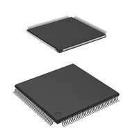
DF2160BVTE10 Renesas Electronics America, DF2160BVTE10 Datasheet - Page 46

DF2160BVTE10
Manufacturer Part Number
DF2160BVTE10
Description
IC H8S MCU FLASH 64K 144TQFP
Manufacturer
Renesas Electronics America
Series
H8® H8S/2100r
Datasheet
1.DF2160BVT10V.pdf
(847 pages)
Specifications of DF2160BVTE10
Core Processor
H8S/2000
Core Size
16-Bit
Speed
10MHz
Connectivity
Host Interface (LPC), I²C, IrDA, SCI, X-Bus
Peripherals
PWM, WDT
Number Of I /o
114
Program Memory Size
64KB (64K x 8)
Program Memory Type
FLASH
Ram Size
4K x 8
Voltage - Supply (vcc/vdd)
2.7 V ~ 3.6 V
Data Converters
A/D 8x10b; D/A 2x8b
Oscillator Type
Internal
Operating Temperature
-20°C ~ 75°C
Package / Case
144-TQFP, 144-VQFP
Lead Free Status / RoHS Status
Contains lead / RoHS non-compliant
Eeprom Size
-
Other names
HD64F2160BVTE10
HD64F2160BVTE10
HD64F2160BVTE10
- Current page: 46 of 847
- Download datasheet (5Mb)
Figure 16.28 IRIC Setting Timing and SCL Control (3)........................................................... 470
Figure 16.29 Block Diagram of Noise Canceler ....................................................................... 473
Figure 16.30 Notes on Reading Master Receive Data............................................................... 479
Figure 16.31 Flowchart for Start Condition Issuance Instruction for Retransmission
Figure 16.32 Stop Condition Issuance Timing.......................................................................... 482
Figure 16.33 IRIC Flag Clear Timing on WAIT Operation...................................................... 483
Figure 16.34 IRIC Flag Clearing Timing When WAIT = 1 ...................................................... 484
Figure 16.35 ICDR Read and ICCR Access Timing in Slave Transmit Mode ......................... 485
Figure 16.36 TRS Bit Set Timing in Slave Mode ..................................................................... 486
Figure 16.37 Diagram of Erroneous Operation when Arbitration is Lost ................................. 487
Section 17 Keyboard Buffer Controller
Figure 17.1
Figure 17.2
Figure 17.3
Figure 17.4
Figure 17.5 (1) Sample Transmit Processing Flowchart.............................................................. 498
Figure 17.5 (2) Sample Transmit Processing Flowchart.............................................................. 499
Figure 17.6
Figure 17.7 (1) Sample Receive Abort Processing Flowchart ..................................................... 501
Figure 17.7 (2) Sample Receive Abort Processing Flowchart ..................................................... 502
Figure 17.8
Figure 17.9
Figure 17.10 KCLKO and KDO Write Timing......................................................................... 504
Figure 17.11 KBF Setting and KCLK Automatic I/O Inhibit Generation Timing.................... 505
Figure 17.12 Receive Counter and KBBR Data Load Timing.................................................. 506
Figure 17.13 Example of KCLK Input Fall Interrupt Operation............................................... 507
Figure 17.14 KBIOE Setting and KCLK Falling Edge Detection Timing................................ 508
Section 18 Host Interface X-Bus Interface (XBS)
Figure 18.1
Figure 18.2
Figure 18.3
Section 19 Host Interface LPC Interface (LPC)
Figure 19.1
Figure 19.2
Figure 19.3
Figure 19.4
Rev. 3.00 Mar 21, 2006 page xliv of liv
and Timing........................................................................................................... 481
Block Diagram of Keyboard Buffer Controller ................................................... 490
Keyboard Buffer Controller Connection.............................................................. 491
Sample Receive Processing Flowchart ................................................................ 496
Receive Timing.................................................................................................... 497
Receive Abort and Transmit Start (Transmission/Reception Switchover)
Timing.................................................................................................................. 502
KCLKI and KDI Read Timing............................................................................. 503
Block Diagram of XBS........................................................................................ 510
GA20 Output........................................................................................................ 522
HIRQ Output Flowchart (Example of Channels 1 and 2) .................................... 526
Block Diagram of LPC ........................................................................................ 530
Typical LFRAME Timing ................................................................................... 564
Abort Mechanism ................................................................................................ 564
GA20 Output........................................................................................................ 566
Transmit Timing ................................................................................................. 500
Related parts for DF2160BVTE10
Image
Part Number
Description
Manufacturer
Datasheet
Request
R

Part Number:
Description:
KIT STARTER FOR M16C/29
Manufacturer:
Renesas Electronics America
Datasheet:

Part Number:
Description:
KIT STARTER FOR R8C/2D
Manufacturer:
Renesas Electronics America
Datasheet:

Part Number:
Description:
R0K33062P STARTER KIT
Manufacturer:
Renesas Electronics America
Datasheet:

Part Number:
Description:
KIT STARTER FOR R8C/23 E8A
Manufacturer:
Renesas Electronics America
Datasheet:

Part Number:
Description:
KIT STARTER FOR R8C/25
Manufacturer:
Renesas Electronics America
Datasheet:

Part Number:
Description:
KIT STARTER H8S2456 SHARPE DSPLY
Manufacturer:
Renesas Electronics America
Datasheet:

Part Number:
Description:
KIT STARTER FOR R8C38C
Manufacturer:
Renesas Electronics America
Datasheet:

Part Number:
Description:
KIT STARTER FOR R8C35C
Manufacturer:
Renesas Electronics America
Datasheet:

Part Number:
Description:
KIT STARTER FOR R8CL3AC+LCD APPS
Manufacturer:
Renesas Electronics America
Datasheet:

Part Number:
Description:
KIT STARTER FOR RX610
Manufacturer:
Renesas Electronics America
Datasheet:

Part Number:
Description:
KIT STARTER FOR R32C/118
Manufacturer:
Renesas Electronics America
Datasheet:

Part Number:
Description:
KIT DEV RSK-R8C/26-29
Manufacturer:
Renesas Electronics America
Datasheet:

Part Number:
Description:
KIT STARTER FOR SH7124
Manufacturer:
Renesas Electronics America
Datasheet:

Part Number:
Description:
KIT STARTER FOR H8SX/1622
Manufacturer:
Renesas Electronics America
Datasheet:

Part Number:
Description:
KIT DEV FOR SH7203
Manufacturer:
Renesas Electronics America
Datasheet:


