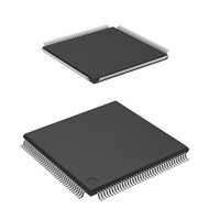
DF2160BVTE10 Renesas Electronics America, DF2160BVTE10 Datasheet - Page 260

DF2160BVTE10
Manufacturer Part Number
DF2160BVTE10
Description
IC H8S MCU FLASH 64K 144TQFP
Manufacturer
Renesas Electronics America
Series
H8® H8S/2100r
Datasheet
1.DF2160BVT10V.pdf
(847 pages)
Specifications of DF2160BVTE10
Core Processor
H8S/2000
Core Size
16-Bit
Speed
10MHz
Connectivity
Host Interface (LPC), I²C, IrDA, SCI, X-Bus
Peripherals
PWM, WDT
Number Of I /o
114
Program Memory Size
64KB (64K x 8)
Program Memory Type
FLASH
Ram Size
4K x 8
Voltage - Supply (vcc/vdd)
2.7 V ~ 3.6 V
Data Converters
A/D 8x10b; D/A 2x8b
Oscillator Type
Internal
Operating Temperature
-20°C ~ 75°C
Package / Case
144-TQFP, 144-VQFP
Lead Free Status / RoHS Status
Contains lead / RoHS non-compliant
Eeprom Size
-
Other names
HD64F2160BVTE10
HD64F2160BVTE10
HD64F2160BVTE10
- Current page: 260 of 847
- Download datasheet (5Mb)
Section 8 I/O Ports
Note:
8.11
Port A is an 8-bit I/O port. Port A pins also function as keyboard buffer controller I/O pins, key-
sense interrupt input pins, expansion A/D converter input pins, and address output pins. Port A pin
functions change according to the operating mode. Port A input/output operates by VccB power
independent from the Vcc power. Up to 5 V can be applied to port A pins if VccB power is 5 V.
Port A has the following registers. PADDR and PAPIN have the same address.
Rev. 3.00 Mar 21, 2006 page 204 of 788
REJ09B0300-0300
Operating
Mode
ABW
HI12E
FGA20E
CS2E
P90DDR
Pin Function
P90/LWR/IRQ2/ADTRG/ECS2
The pin function is switched as shown below according to the combination of operating mode,
the ABW bit in WSCR, the HI12E and CS2E bits in SYSCR2, the FGA20E bit in HICR, and
the P90DDR bit.
Port A data direction register (PADDR)
Port A output data register (PAODR)
Port A input data register (PAPIN)
* When the IRQ2E bit in IER is set to 1 in mode 1, 2, or 3 (EXPE = 1) with the ABW bit in
Port A
WSCR set to 1, or in mode 2 and 3 (EXPE = 0), this pin is used as the IRQ2 input pin.
When TRGS1 and TRGS0 in ADCR of the A/D converter are both set to 1, this pin is
used as the ADTRG input pin.
LWR output
pin
—
0
Modes 1, 2, 3 (EXPE = 1)
input pin
P90
—
—
—
0
1
P90 output
IRQ2 input pin, ADTRG input pin *
pin
1
input pin
P90
0
Any one 0
Modes 2, 3 (EXPE = 0)
P90 output
pin
—
1
ECS2 input
pin
—
1
1
1
Related parts for DF2160BVTE10
Image
Part Number
Description
Manufacturer
Datasheet
Request
R

Part Number:
Description:
KIT STARTER FOR M16C/29
Manufacturer:
Renesas Electronics America
Datasheet:

Part Number:
Description:
KIT STARTER FOR R8C/2D
Manufacturer:
Renesas Electronics America
Datasheet:

Part Number:
Description:
R0K33062P STARTER KIT
Manufacturer:
Renesas Electronics America
Datasheet:

Part Number:
Description:
KIT STARTER FOR R8C/23 E8A
Manufacturer:
Renesas Electronics America
Datasheet:

Part Number:
Description:
KIT STARTER FOR R8C/25
Manufacturer:
Renesas Electronics America
Datasheet:

Part Number:
Description:
KIT STARTER H8S2456 SHARPE DSPLY
Manufacturer:
Renesas Electronics America
Datasheet:

Part Number:
Description:
KIT STARTER FOR R8C38C
Manufacturer:
Renesas Electronics America
Datasheet:

Part Number:
Description:
KIT STARTER FOR R8C35C
Manufacturer:
Renesas Electronics America
Datasheet:

Part Number:
Description:
KIT STARTER FOR R8CL3AC+LCD APPS
Manufacturer:
Renesas Electronics America
Datasheet:

Part Number:
Description:
KIT STARTER FOR RX610
Manufacturer:
Renesas Electronics America
Datasheet:

Part Number:
Description:
KIT STARTER FOR R32C/118
Manufacturer:
Renesas Electronics America
Datasheet:

Part Number:
Description:
KIT DEV RSK-R8C/26-29
Manufacturer:
Renesas Electronics America
Datasheet:

Part Number:
Description:
KIT STARTER FOR SH7124
Manufacturer:
Renesas Electronics America
Datasheet:

Part Number:
Description:
KIT STARTER FOR H8SX/1622
Manufacturer:
Renesas Electronics America
Datasheet:

Part Number:
Description:
KIT DEV FOR SH7203
Manufacturer:
Renesas Electronics America
Datasheet:


