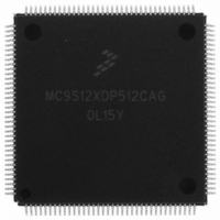
MC9S12XDP512CAG Freescale Semiconductor, MC9S12XDP512CAG Datasheet - Page 1167

MC9S12XDP512CAG
Manufacturer Part Number
MC9S12XDP512CAG
Description
IC MCU 512K FLASH 144-LQFP
Manufacturer
Freescale Semiconductor
Series
HCS12r
Datasheet
1.MC9S12XD64CAA.pdf
(1348 pages)
Specifications of MC9S12XDP512CAG
Core Processor
HCS12X
Core Size
16-Bit
Speed
80MHz
Connectivity
CAN, EBI/EMI, I²C, IrDA, LIN, SCI, SPI
Peripherals
LVD, POR, PWM, WDT
Number Of I /o
119
Program Memory Size
512KB (512K x 8)
Program Memory Type
FLASH
Eeprom Size
4K x 8
Ram Size
32K x 8
Voltage - Supply (vcc/vdd)
2.35 V ~ 5.5 V
Data Converters
A/D 24x10b
Oscillator Type
External
Operating Temperature
-40°C ~ 85°C
Package / Case
144-LQFP
Processor Series
S12XD
Core
HCS12
Data Bus Width
16 bit
Data Ram Size
32 KB
Interface Type
CAN/I2C/SCI/SPI
Maximum Clock Frequency
40 MHz
Number Of Programmable I/os
119
Number Of Timers
12
Maximum Operating Temperature
+ 85 C
Mounting Style
SMD/SMT
3rd Party Development Tools
EWHCS12
Development Tools By Supplier
EVB9S12XDP512E
Minimum Operating Temperature
- 40 C
On-chip Adc
2 (24-ch x 10-bit)
Cpu Family
HCS12
Device Core Size
16b
Frequency (max)
40MHz
Total Internal Ram Size
32KB
# I/os (max)
119
Number Of Timers - General Purpose
12
Operating Supply Voltage (typ)
2.5/5V
Operating Supply Voltage (max)
2.75/5.5V
Operating Supply Voltage (min)
2.35/3.15V
Instruction Set Architecture
CISC
Operating Temp Range
-40C to 85C
Operating Temperature Classification
Industrial
Mounting
Surface Mount
Pin Count
144
Package Type
LQFP
For Use With
DEMO9S12XDT512E - BOARD DEMO FOR MC9S12XDT512EVB9S12XDP512E - BOARD DEMO FOR MC9S12XDP512
Lead Free Status / RoHS Status
Lead free / RoHS Compliant
Available stocks
Company
Part Number
Manufacturer
Quantity
Price
Company:
Part Number:
MC9S12XDP512CAG
Manufacturer:
Freescale Semiconductor
Quantity:
10 000
Part Number:
MC9S12XDP512CAG
Manufacturer:
FREESCLA
Quantity:
20 000
- Current page: 1167 of 1348
- Download datasheet (8Mb)
28.4.1.2
The Flash command controller is used to supervise the command write sequence to execute program,
erase, erase verify, erase abort, and data compress algorithms.
Before starting a command write sequence, the ACCERR and PVIOL flags in the FSTAT register must be
clear (see
determine the state of the address, data and command buffers. If the CBEIF flag is set, indicating the
buffers are empty, a new command write sequence can be started. If the CBEIF flag is clear, indicating the
buffers are not available, a new command write sequence will overwrite the contents of the address, data
and command buffers.
A command write sequence consists of three steps which must be strictly adhered to with writes to the
Flash module not permitted between the steps. However, Flash register and array reads are allowed during
a command write sequence. The basic command write sequence is as follows:
The address written in step 1 will be stored in the FADDR registers and the data will be stored in the
FDATA registers. If the CBEIF flag in the FSTAT register is clear when the first Flash array write occurs,
the contents of the address and data buffers will be overwritten and the CBEIF flag will be set. When the
CBEIF flag is cleared, the CCIF flag is cleared on the same bus cycle by the Flash command controller
indicating that the command was successfully launched. For all command write sequences except data
compress and sector erase abort, the CBEIF flag will set four bus cycles after the CCIF flag is cleared
indicating that the address, data, and command buffers are ready for a new command write sequence to
begin. For data compress and sector erase abort operations, the CBEIF flag will remain clear until the
operation completes. Except for the sector erase abort command, a buffered command will wait for the
active operation to be completed before being launched. The sector erase abort command is launched when
the CBEIF flag is cleared as part of a sector erase abort command write sequence. Once a command is
launched, the completion of the command operation is indicated by the setting of the CCIF flag in the
FSTAT register. The CCIF flag will set upon completion of all active and buffered commands.
28.4.2
Table 28-18
block.
Freescale Semiconductor
1. Write to a valid address in the Flash memory. Addresses in multiple Flash blocks can be written to
2. Write a valid command to the FCMD register.
3. Clear the CBEIF flag in the FSTAT register by writing a 1 to CBEIF to launch the command.
FCMDB
0x05
as long as the location is at the same relative address in each available Flash block. Multiple
addresses must be written in Flash block order starting with the lower Flash block.
Section 28.3.2.6, “Flash Status Register
Flash Commands
summarizes the valid Flash commands along with the effects of the commands on the Flash
Command Write Sequence
Command
Erase
Verify
NVM
Verify all memory bytes in the Flash block are erased.
If the Flash block is erased, the BLANK flag in the FSTAT register will set upon command
completion.
Table 28-18. Flash Command Description
MC9S12XDP512 Data Sheet, Rev. 2.21
(FSTAT)”) and the CBEIF flag should be tested to
Function on Flash Memory
Chapter 28 256 Kbyte Flash Module (S12XFTX256K2V1)
1169
Related parts for MC9S12XDP512CAG
Image
Part Number
Description
Manufacturer
Datasheet
Request
R

Part Number:
Description:
16-BIT MICROPROCESSOR FAMILY
Manufacturer:
FREESCALE [Freescale Semiconductor, Inc]
Datasheet:
Part Number:
Description:
Manufacturer:
Freescale Semiconductor, Inc
Datasheet:
Part Number:
Description:
Manufacturer:
Freescale Semiconductor, Inc
Datasheet:
Part Number:
Description:
Manufacturer:
Freescale Semiconductor, Inc
Datasheet:
Part Number:
Description:
Manufacturer:
Freescale Semiconductor, Inc
Datasheet:
Part Number:
Description:
Manufacturer:
Freescale Semiconductor, Inc
Datasheet:
Part Number:
Description:
Manufacturer:
Freescale Semiconductor, Inc
Datasheet:
Part Number:
Description:
Manufacturer:
Freescale Semiconductor, Inc
Datasheet:
Part Number:
Description:
Manufacturer:
Freescale Semiconductor, Inc
Datasheet:
Part Number:
Description:
Manufacturer:
Freescale Semiconductor, Inc
Datasheet:
Part Number:
Description:
Manufacturer:
Freescale Semiconductor, Inc
Datasheet:
Part Number:
Description:
Manufacturer:
Freescale Semiconductor, Inc
Datasheet:
Part Number:
Description:
Manufacturer:
Freescale Semiconductor, Inc
Datasheet:
Part Number:
Description:
Manufacturer:
Freescale Semiconductor, Inc
Datasheet:
Part Number:
Description:
Manufacturer:
Freescale Semiconductor, Inc
Datasheet:


