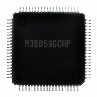
M38D59GCHP#U0 Renesas Electronics America, M38D59GCHP#U0 Datasheet - Page 9

M38D59GCHP#U0
Manufacturer Part Number
M38D59GCHP#U0
Description
IC 740/38D5 MCU QZ-ROM 80LQFP
Manufacturer
Renesas Electronics America
Series
740/38000r
Datasheet
1.M38D58G8FPU0.pdf
(144 pages)
Specifications of M38D59GCHP#U0
Core Processor
740
Core Size
8-Bit
Speed
12.5MHz
Connectivity
SIO, UART/USART
Peripherals
LCD, LED, PWM, WDT
Number Of I /o
59
Program Memory Size
48KB (48K x 8)
Program Memory Type
QzROM
Ram Size
2K x 8
Voltage - Supply (vcc/vdd)
1.8 V ~ 5.5 V
Data Converters
A/D 8x10b
Oscillator Type
Internal
Operating Temperature
-20°C ~ 85°C
Package / Case
80-LQFP
Lead Free Status / RoHS Status
Lead free / RoHS Compliant
Eeprom Size
-
Available stocks
Company
Part Number
Manufacturer
Quantity
Price
38D5 Group
Rev.3.04
REJ03B0158-0304
PIN DESCRIPTION
Table 3
V
RESET
X
X
V
COM
COM
COM
COM
P0
P0
P1
P1
P2
P2
P2
P2
P3
P3
P4
P4
P4
P4
P4
P4
P4
P4
CC
IN
OUT
L1,
0
7
0
7
0
3
4
7
0
7
0
1
2
3
4
5
6
7
/SEG
/SEG
/SEG
/SEG
/SEG
/SEG
/SEG
/SEG
/SEG
/SEG
/R
/T
/S
/S
/S
/S
/S
/S
, V
V
0
3
4
7
L2,
X
CLK1
RDY1
IN2
OUT2
CLK2
RDY2
X
−
/SEG
/SEG
SS
D
D
Pin
/(KW
V
8
15
16
23
0
3
4
7
24
31
−
/(KW
/(KW
−
/(KW
L3
/(KW
/(KW
−
−
Pin description (1)
35
32
−
0
May 20, 2008 Page 7 of 134
)
4
7
2
1
3
)−
)
)
)
)
Power source
Reset input
Clock input
Clock output
LCD power
source
Common output
Common output
Segment output
I/O port P0
I/O port P1
I/O port P2
I/O port P3
I/O port P4
Name
• Apply power source voltage to V
• Reset input pin for active “L”.
• Input and output pins for the main clock generating circuit.
• Connect a ceramic resonator or a quartz-crystal oscillator between the X
• Feedback resistor is built in between X
• Input 0 ≤ V
• Input 0 − V
• LCD common output pins.
• COM
• COM
• LCD common/segment output pins.
• 8-bit I/O port.
• CMOS compatible input level.
• CMOS 3-state output structure.
• I/O direction register allows each pin to be
• Pull-up control is enabled in a bit unit.
• 8-bit I/O port.
• CMOS compatible input level.
• CMOS 3-state output structure.
• I/O direction register allows each pin to be
• Pull-up control is enabled in 4-bit unit.
• 8-bit I/O port.
• CMOS compatible input level.
• CMOS 3-state output structure.
• I/O direction register allows each pin to be
• Pull-up control is enabled in 4-bit unit.
set the oscillation frequency. When an external clock is used, connect the clock source to
X
individually programmed as either input or output.
programmed as either input or output.
individually programmed as either input or output.
individually programmed as either input or output.
individually programmed as either input or output.
IN
, and leave X
2
3
and COM
is not used at 1/3 duty ratio.
L1
L3
≤ V
voltage to LCD.
OUT
3
L2
are not used at 1/2 duty ratio.
≤ V
Function
pin open.
L3
voltage.
CC
, and 0 V to V
IN
pin and X
SS
OUT
.
• Serial I/O1 function pins
• Serial I/O2
function pins
pin.
Function except a port function
• Key input interrupt
• Key input interrupt
IN
input pins
input pins
and X
OUT
pins to


