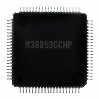
M38D59GCHP#U0 Renesas Electronics America, M38D59GCHP#U0 Datasheet - Page 40

M38D59GCHP#U0
Manufacturer Part Number
M38D59GCHP#U0
Description
IC 740/38D5 MCU QZ-ROM 80LQFP
Manufacturer
Renesas Electronics America
Series
740/38000r
Datasheet
1.M38D58G8FPU0.pdf
(144 pages)
Specifications of M38D59GCHP#U0
Core Processor
740
Core Size
8-Bit
Speed
12.5MHz
Connectivity
SIO, UART/USART
Peripherals
LCD, LED, PWM, WDT
Number Of I /o
59
Program Memory Size
48KB (48K x 8)
Program Memory Type
QzROM
Ram Size
2K x 8
Voltage - Supply (vcc/vdd)
1.8 V ~ 5.5 V
Data Converters
A/D 8x10b
Oscillator Type
Internal
Operating Temperature
-20°C ~ 85°C
Package / Case
80-LQFP
Lead Free Status / RoHS Status
Lead free / RoHS Compliant
Eeprom Size
-
Available stocks
Company
Part Number
Manufacturer
Quantity
Price
38D5 Group
Rev.3.04
REJ03B0158-0304
16-bit Timer
Read and write operation on 16-bit timer must be performed for
both high and low-order bytes. When reading a 16-bit timer, read
the high-order byte first. When writing to a 16-bit timer, write
the low-order byte first. The 16-bit timer cannot perform the
correct operation when reading during the write operation, or
when writing during the read operation.
Fig. 28 Timer X block diagram
Data for control of event counter window
φSOURCE
CNTR
(1)
0
May 20, 2008 Page 38 of 134
Frequency divider
P6
P6
INT
5
/T
3
Timer 1 interrupt
/T
INT
Xc
XOUT1
10
XOUT2
Both edges
Clock for Timer X
IN
detection
/INT
00
INT
/INT
/(LED
/(LED
11
2
01
CNTR
edge switch bits
3
“00”
)
1
“01”
)
“10”
“11”
Note1: φSOURCE indicates the followings:
Edge
selection
Edge
selection
0
Edge
selection
2
active
Timer X output
control bit 1
“0”
•X
•On-chip oscillator divided by 4 in the on-chip oscillator mode
•Sub-clock in the low-speed mode
“1”
Latch
P6
direction
register
P6
direction
register
IN
D Q
Timer X output
control bit 2
Timer X frequency
division selection bits
3
5
input in the frequency/2, 4, or 8 mode
Timer X count source selection bit
measurement
Timer X output 1
selection bit
Timer X output 2
selection bit
Pulse width
Timer X operating
mode bits
Noise filter
(4 times same
levels judgment)
mode
Timer X operating
mode bits
“100”
P6
latch
P6
latch
“000”
“001”
“010”
“011”
“101”
5
3
Frequency
divider
Timer X count
detection
X
Timer X output 1
active edge switch
bit
stop bit
IN
Edge
“0”
“1”
“0”
“1”
Timer X output 2
active edge
switch bit
“010”
1/4
Timer X write
1/2
Noise filter sampling
clock selection bit
control bit
IGBT output mode
PWM mode
“0”
“1”
Compare register 3 (low-order)(8) Compare register 3 (high-order)(8)
Compare register 1 (low-order)(8) Compare register 1 (high-order)(8)
Compare register 2 (low-order)(8) Compare register 2 (high-order)(8)
Delay
circuit
Timer X (low-order) latch (8)
Timer X (low-order)(8)
Q
Q
Q
Q
0 µs
4/f(X
8/f(X
16/f(X
R
S
“1”
IN
IN
“0”
T
Q
Q
T
IN
External trigger delay time
selection bits
Pulse output mode
)
)
Trigger for IGBT input control bit
)
R
“00”
“01”
“10”
“11”
T
× 2
Timer X (high-order) latch (8)
Timer X (high-order)(8)
Delay circuit 1/2
Trigger for IGBT input control bit
“1”
“0”
Extend counter (2)
Extend latch (2)
“000”
“001”
“011”
“100”
“101”
“010”
Equal
Timer X operating
mode bits
Data bus
INT
interrupt request
Timer X interrupt
request
CNTR
interrupt request
0
0


