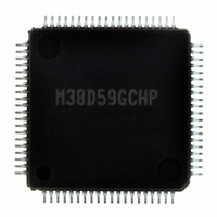
M38D59GCHP#U0 Renesas Electronics America, M38D59GCHP#U0 Datasheet - Page 34

M38D59GCHP#U0
Manufacturer Part Number
M38D59GCHP#U0
Description
IC 740/38D5 MCU QZ-ROM 80LQFP
Manufacturer
Renesas Electronics America
Series
740/38000r
Datasheet
1.M38D58G8FPU0.pdf
(144 pages)
Specifications of M38D59GCHP#U0
Core Processor
740
Core Size
8-Bit
Speed
12.5MHz
Connectivity
SIO, UART/USART
Peripherals
LCD, LED, PWM, WDT
Number Of I /o
59
Program Memory Size
48KB (48K x 8)
Program Memory Type
QzROM
Ram Size
2K x 8
Voltage - Supply (vcc/vdd)
1.8 V ~ 5.5 V
Data Converters
A/D 8x10b
Oscillator Type
Internal
Operating Temperature
-20°C ~ 85°C
Package / Case
80-LQFP
Lead Free Status / RoHS Status
Lead free / RoHS Compliant
Eeprom Size
-
Available stocks
Company
Part Number
Manufacturer
Quantity
Price
38D5 Group
Rev.3.04
REJ03B0158-0304
<Notes>
The interrupt request bit may be set to “1” in the following cases.
• When setting the external interrupt active edge
• When switching the interrupt sources of an interrupt vector
• When switching the INT pins
Fig. 22 Timing of interrupt request generation, interrupt request bit, and interrupt acceptance
Related bits: INT
address where two or more interrupt sources are assigned
Related bit:
Related bits: INT
Internal clock φ
SYNC
May 20, 2008 Page 32 of 134
(bit 0 of interrupt edge selection register
(address 003A
INT
(bit 1 of interrupt edge selection register)
INT
(bit 2 of interrupt edge selection register)
CNTR
(bits 6 and 7 of timer X control register 1
(address 002E
CNTR
(bits 6 of timer Y mode register
(address 0038
Timer Y/CNTR
INT
(bit 3 of interrupt edge selection register)
(bit 4 of interrupt edge selection register)
(bit 5 of interrupt edge selection register)
(1) The interrupt request bit for an interrupt request generated during period 1 is set to “1” at timing point IR1.
(2) The interrupt request bit for an interrupt request generated during period 2 is set to “1” at timing point IR1 or IR2.
0
1
2
0
1
The timing point at which the bit is set to “1” varies depending on conditions. When two or more interrupt
requests are generated during the period 2, each request bit may be set to “1” at timing point IR1 or IR2
separately.
interrupt edge selection bit
interrupt edge selection bit
interrupt edge selection bit
input port switch bit
input port switch bit
0
1
activate edge switch bit
activate edge switch bit
T1 T2 T3 : Interrupt acceptance timing points
IR1 IR2 : Timings points at which the interrupt request bit is set to “1”.
Note : Period 2 indicates the last φ cycle during one instruction cycle.
T1
16
16
16
))
1
))
))
interrupt switch bit
Instruction cycle
1
2
IR1 T2
If it is not necessary to generate an interrupt synchronized with
these settings, take the following sequence.
(1) Set the corresponding enable bit to “0” (disabled).
(2) Set the interrupt edge selection bit (the active edge switch
(3) Set the corresponding interrupt request bit to “0” after one
(4) Set the corresponding interrupt enable bit to “1” (enabled).
Push onto stack
Vector fetch
bit) or the interrupt source bit.
or more instructions have been executed.
IR2 T3
Instruction cycle


