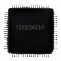
M38D59GCHP#U0 Renesas Electronics America, M38D59GCHP#U0 Datasheet - Page 35

M38D59GCHP#U0
Manufacturer Part Number
M38D59GCHP#U0
Description
IC 740/38D5 MCU QZ-ROM 80LQFP
Manufacturer
Renesas Electronics America
Series
740/38000r
Datasheet
1.M38D58G8FPU0.pdf
(144 pages)
Specifications of M38D59GCHP#U0
Core Processor
740
Core Size
8-Bit
Speed
12.5MHz
Connectivity
SIO, UART/USART
Peripherals
LCD, LED, PWM, WDT
Number Of I /o
59
Program Memory Size
48KB (48K x 8)
Program Memory Type
QzROM
Ram Size
2K x 8
Voltage - Supply (vcc/vdd)
1.8 V ~ 5.5 V
Data Converters
A/D 8x10b
Oscillator Type
Internal
Operating Temperature
-20°C ~ 85°C
Package / Case
80-LQFP
Lead Free Status / RoHS Status
Lead free / RoHS Compliant
Eeprom Size
-
Available stocks
Company
Part Number
Manufacturer
Quantity
Price
- Current page: 35 of 144
- Download datasheet (3Mb)
38D5 Group
Rev.3.04
REJ03B0158-0304
• Key Input Interrupt (Key-on Wake-Up)
A key input interrupt request is generated by detecting the falling
edge from any pin of ports P2
to input mode. In other words, it is generated when AND of input
level goes from “1” to “0”. An example of using a key input
Fig. 23 Connection example when using key input interrupt
May 20, 2008 Page 33 of 134
P2
P2
P2
P2
2
1
P4
P4
P4
P4
3
0
output
output
output
output
7
6
5
4
input
input
input
input
Port PXx
“L” level output
0
−P2
∗
∗
∗
∗
∗
∗
∗
∗
3
, P4
Segment output
disable register 1
Bit 0 = “1”
Segment output
disable register 1
Bit 3 = “1”
Segment output
disable register 1
Bit 2 = “1”
Segment output
disable register 1
Bit 1 = “1”
PULL register 3
Bit 1 = “1”
4
−P4
∗∗
∗∗
∗∗
∗∗
∗∗
∗∗
∗∗
∗∗
7
that have been set
Port P4 direction
register bit 7 = “0”
Port P4 direction
register bit 5 = “0”
Port P4 direction
register bit 4 = “0”
Port P4 direction
register bit 6 = “0”
Port P4
latch
Port P4
latch
Port P4
latch
Port P2
latch
Port P2
latch
Port P2
latch
Port P2
latch
Port P4
latch
Port P2 direction
register bit 3 = “1”
Port P2
register bit 2 = “1”
Port P2 direction
register bit 1 = “1”
Port P2 direction
register bit 0 = “1”
4
2
6
5
3
1
0
7
2
Key input control
register bit 2 = “1”
Key input control
register bit 3 = “1”
Key input control
register bit 7 = “1”
direction
Key input control
register bit 4 = “1”
Key input control
register bit 5 = “1”
Key input control
register bit 1 = “1”
Key input control
register bit 6 = “1”
Key input control
register bit 0 = “1”
interrupt is shown in Figure 23, where an interrupt request is
generated by pressing one of the keys consisted as an active-low
key matrix which inputs to ports P4
∗∗ CMOS output buffer
∗ P-channel transistor for pull-up
4
−P4
Key input interrupt request
7
.
Port P4
Input reading circuit
Port P2
Input reading circuit
Related parts for M38D59GCHP#U0
Image
Part Number
Description
Manufacturer
Datasheet
Request
R

Part Number:
Description:
KIT STARTER FOR M16C/29
Manufacturer:
Renesas Electronics America
Datasheet:

Part Number:
Description:
KIT STARTER FOR R8C/2D
Manufacturer:
Renesas Electronics America
Datasheet:

Part Number:
Description:
R0K33062P STARTER KIT
Manufacturer:
Renesas Electronics America
Datasheet:

Part Number:
Description:
KIT STARTER FOR R8C/23 E8A
Manufacturer:
Renesas Electronics America
Datasheet:

Part Number:
Description:
KIT STARTER FOR R8C/25
Manufacturer:
Renesas Electronics America
Datasheet:

Part Number:
Description:
KIT STARTER H8S2456 SHARPE DSPLY
Manufacturer:
Renesas Electronics America
Datasheet:

Part Number:
Description:
KIT STARTER FOR R8C38C
Manufacturer:
Renesas Electronics America
Datasheet:

Part Number:
Description:
KIT STARTER FOR R8C35C
Manufacturer:
Renesas Electronics America
Datasheet:

Part Number:
Description:
KIT STARTER FOR R8CL3AC+LCD APPS
Manufacturer:
Renesas Electronics America
Datasheet:

Part Number:
Description:
KIT STARTER FOR RX610
Manufacturer:
Renesas Electronics America
Datasheet:

Part Number:
Description:
KIT STARTER FOR R32C/118
Manufacturer:
Renesas Electronics America
Datasheet:

Part Number:
Description:
KIT DEV RSK-R8C/26-29
Manufacturer:
Renesas Electronics America
Datasheet:

Part Number:
Description:
KIT STARTER FOR SH7124
Manufacturer:
Renesas Electronics America
Datasheet:

Part Number:
Description:
KIT STARTER FOR H8SX/1622
Manufacturer:
Renesas Electronics America
Datasheet:

Part Number:
Description:
KIT DEV FOR SH7203
Manufacturer:
Renesas Electronics America
Datasheet:


